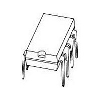
ICM7555CN/01.112 NXP Semiconductors, ICM7555CN/01.112 Datasheet - Page 3

ICM7555CN/01.112
Manufacturer Part Number
ICM7555CN/01.112
Description
Manufacturer
NXP Semiconductors
Type
Standardr
Datasheet
1.ICM7555CN01.112.pdf
(22 pages)
Specifications of ICM7555CN/01.112
# Internal Timers
1
Power Dissipation
1.16W
Operating Supply Voltage (min)
3V
Operating Supply Voltage (typ)
3.3/5/9/12/15V
Operating Supply Voltage (max)
16V
Package Type
PDIP
High Level Output Current
-1mA
Low Level Output Current
3.2mA
Pin Count
8
Operating Temp Range
0C to 70C
Operating Temperature Classification
Commercial
Mounting
Through Hole
Lead Free Status / RoHS Status
Compliant
NXP Semiconductors
6. Pinning information
7. Functional description
ICM7555_2
Product data sheet
Fig 2.
TRIGGER
OUTPUT
RESET
Pin configuration for SO8
GND
1
2
3
4
6.1 Pinning
6.2 Pin description
7.1 Function selection
ICM7555CD
ICM7555ID
Table 2.
Refer to
Table 3.
[1]
002aae400
Symbol
GND
TRIGGER
OUTPUT
RESET
CONTROL_VOLTAGE
THRESHOLD
DISCHARGE
V
THRESHOLD voltage
don’t care
>
V
don’t care
DD
th
2
3
<
RESET will dominate all other inputs; TRIGGER will dominate over THRESHOLD.
V+
2
3
V+
8
7
6
5
Figure 1 “Functional
V
DISCHARGE
THRESHOLD
CONTROL_VOLTAGE
Pin description
Function selection
DD
Rev. 02 — 3 August 2009
Pin
1
2
3
4
5
6
7
8
TRIGGER voltage
don’t care
>
V
<
trig
1
1
3
3
>
V+
V+
diagram”.
1
3
Description
supply ground
start timer input; (active LOW)
timer logic level output
timer inhibit input; (active LOW)
timing capacitor upper voltage sense input
timing capacitor lower voltage sense input
timing capacitor discharge output
supply voltage
V+
Fig 3.
TRIGGER
OUTPUT
RESET
Pin configuration for DIP8
GND
RESET
L
H
H
H
1
2
3
4
[1]
ICM7555CN
ICM7555IN
002aae401
OUTPUT
L
L
stable
H
General purpose CMOS timer
8
7
6
5
V
DISCHARGE
THRESHOLD
CONTROL_VOLTAGE
DD
Discharge switch
on
on
stable
off
© NXP B.V. 2009. All rights reserved.
ICM7555
3 of 22


