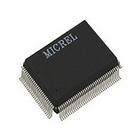
KS8993F A5 Micrel Inc, KS8993F A5 Datasheet - Page 26

KS8993F A5
Manufacturer Part Number
KS8993F A5
Description
Manufacturer
Micrel Inc
Datasheet
1.KS8993F_A5.pdf
(99 pages)
Specifications of KS8993F A5
Number Of Primary Switch Ports
3
Internal Memory Buffer Size
32
Operating Supply Voltage (typ)
1.8/2.5/3.3V
Fiber Support
Yes
Integrated Led Drivers
Yes
Phy/transceiver Interface
MII/SNI
Power Supply Type
Analog/Digital
Package Type
PQFP
Data Rate (typ)
10/100Mbps
Vlan Support
Yes
Operating Temperature (max)
70C
Operating Temperature (min)
0C
Pin Count
128
Mounting
Surface Mount
Jtag Support
No
Operating Supply Voltage (max)
1.89/3.465V
Operating Temperature Classification
Commercial
Lead Free Status / RoHS Status
Not Compliant
KS8993F
To ensure proper operation, a resistive voltage divider is recommended to adjust the fiber transceiver SD output
voltage swing to match the KS8993F FXSD1 input voltage threshold. Refer to KS8993F schematic for recommended
fiber transceiver connections.
2.3.6 100BASE-FX Far-End Fault (FEF)
Far-End Fault (FEF) occurs when the signal detection is logically false on the receive side of the fiber transceiver. The
KS8993F detects a FEF when its FXSD1 input is between 1.0V and 1.8V. When a FEF occurs, the transmission side
signals the link partner by sending 84 ones followed by 1 zero in the idle period between frames.
Upon receiving a FEF, the link will go down (even when the fiber signal is detected) to indicate a fault condition. The
transmitting side is not affected when a FEF is received, and will continue to send out its normal transmit pattern from
the MAC.
By default, FEF is enabled. FEF can be disabled through register setting.
2.3.7
The output 10BASE-T driver is incorporated into the 100BASE-TX driver to allow transmission with the same
magnetic. They are internally wave-shaped and pre-emphasized into outputs with a typical 2.3 V amplitude. The
harmonic contents are at least 27 dB below the fundamental when driven by an all-ones Manchester-encoded signal.
On the receive side, input buffer and level detecting squelch circuits are employed. A differential input receiver circuit
and a PLL perform the decoding function. The Manchester-encoded data stream is separated into clock signal and
NRZ data. A squelch circuit rejects signals with levels less than 400 mV or with short pulse widths in order to prevent
noises at the RXP or RXM input from falsely triggering the decoder. When the input exceeds the squelch limit, the
PLL locks onto the incoming signal and the KS8993F decodes a data frame. The receiver clock is maintained active
during idle periods in between data reception.
2.3.8
The KS8993F features a per-port power down mode. To save power, a port that is not being used can be powered
down through the port control registers, or MIIM control registers. In addition, there is a full chip power down mode.
When activated, the entire chip will be shut down.
2.3.9 Auto MDI/MDI-X Crossover
August 26, 2004
10BASE-T Transmit and Receive
Power Management
FXSD1 (pin 44)
Less than 0.2V
Greater than 1V, but less than 1.8V
Greater than 2.2V
Table 1: FX and TX Mode Selection
- 26 -
Condition
TX mode
FX mode
FX mode
No signal detected;
Far-End Fault generated (if enabled)
Signal detected
Revision 1.0
Micrel


