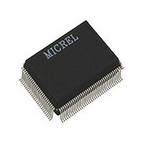
KSZ8995M A4 Micrel Inc, KSZ8995M A4 Datasheet - Page 11

KSZ8995M A4
Manufacturer Part Number
KSZ8995M A4
Description
Manufacturer
Micrel Inc
Datasheet
1.KSZ8995M_A4.pdf
(76 pages)
Specifications of KSZ8995M A4
Number Of Primary Switch Ports
5
Internal Memory Buffer Size
64
Operating Supply Voltage (typ)
1.8/2.5/3.3V
Fiber Support
Yes
Integrated Led Drivers
Yes
Phy/transceiver Interface
MII/SNI
Power Supply Type
Analog/Digital
Package Type
PQFP
Data Rate (typ)
10/100Mbps
Vlan Support
Yes
Operating Temperature (max)
70C
Operating Temperature (min)
0C
Pin Count
128
Mounting
Surface Mount
Jtag Support
No
Operating Supply Voltage (max)
1.9/2.6/3.6V
Operating Supply Voltage (min)
1.7/2.4/3V
Operating Temperature Classification
Commercial
Data Rate
100Mbps
Lead Free Status / RoHS Status
Compliant
Note:
1. P = Power supply
June 2009
KS8995M
Pin Number
I = Input
O = Output
I/O = Bi-directional
Gnd = Ground
Ipu = Input w/ internal pull-up
Ipd = Input w/ internal pull-down
Ipd/O = Input w/ internal pull-down during reset, output pin otherwise
Ipu/O = Input w/ internal pull-up during reset, output pin otherwise
PU = Strap pin pull-up
PD = Strap pin pull-down
Otri = Output tristated
NC = No Connect
59
60
61
62
63
64
65
66
67
68
69
70
71
72
73
74
75
76
77
78
79
80
81
Pin Name
PMRXDV
PMRXER
SMRXDV
PMRXD3
PMRXD2
PMRXD1
PMRXD0
SMTXEN
SMTXER
SMRXD3
SMRXD2
SMTXD3
SMTXD2
SMTXD1
SMTXD0
PMRXC
SMRXC
SMTXC
VDDIO
VDDIO
GNDD
PCRS
PCOL
Type
Ipd/O
Ipd/O
Ipd/O
Ipd/O
Ipd/O
Ipd/O
Ipd/O
Ipd/O
Ipd/O
Ipd/O
Ipd/O
Gnd
Ipd
Ipd
Ipd
Ipd
Ipd
Ipd
I/O
I/O
O
P
P
(1)
Port
5
5
5
5
5
5
5
5
5
Pin Function
3.3V digital V
PHY[5] MII receive clock. PHY mode MII
PHY[5] MII receive data valid
PHY[5] MII receive bit 3. Strap option: PD (default) = enable flow
control; PU = disable flow control.
PHY[5] MII receive bit 2. Strap option: PD (default) = disable back
pressure; PU = enable back pressure.
PHY[5] MII receive bit 1. Strap option: PD (default) = drop excessive
collision packets; PU = does not drop excessive collision packets.
PHY[5] MII receive bit 0. Strap option: PD (default) = disable
aggressive back-off algorithm in half-duplex mode; PU = enable for
performance enhancement.
PHY[5] MII receive error. Strap option: PD (default) = 1522/1518 bytes;
PU = packet size up to 1536 bytes.
PHY[5] MII carrier sense. Strap option for port 4 only. See “Register 76.”
PD (default) = Force half-duplex if auto-negotiation is disabled or fails.
PU = Force full-duplex if auto-negotiation is disabled or fails.
PHY[5] MII collision detect. Strap option for port 4 only.
See “Register 66.” PD (default) = No force flow control. PU = Force
flow control.
Switch MII transmit enable
Switch MII transmit bit 3
Switch MII transmit bit 2
Switch MII transmit bit 1
Switch MII transmit bit 0
Switch MII transmit error
Switch MII transmit clock. Input in MAC mode, output in PHY mode MII.
Digital ground
3.3V digital V
Switch MII receive clock. Input in MAC mode, output in PHY mode MII.
Switch MII receive data valid
Switch MII receive bit 3. Strap option: PD (default) = Disable Switch MII
full-duplex flow control; PU = Enable Switch MII full-duplex flow control.
Switch MII receive bit 2. Strap option: PD (default) = Switch MII in full-
duplex mode; PU = Switch MII in half-duplex mode.
11
DD
DD
for digital I/O circuitry
for digital I/O circuitry
M9999-062309
Micrel, Inc.


