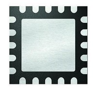
PIC16F1507-I/ML Microchip Technology, PIC16F1507-I/ML Datasheet - Page 11

PIC16F1507-I/ML
Manufacturer Part Number
PIC16F1507-I/ML
Description
3.5KB Flash, 128B RAM, 18 I/O, CLC, CWG, DDS, 10-bit ADC 20 QFN 4x4mm TUBE
Manufacturer
Microchip Technology
Series
PIC® 16Fr
Datasheets
1.PIC16F1507-EML.pdf
(266 pages)
2.PIC16F1507-EML.pdf
(26 pages)
3.PIC16F1507-EML.pdf
(40 pages)
Specifications of PIC16F1507-I/ML
Processor Series
PIC16
Core
PIC16F
Data Bus Width
8 bit
Program Memory Type
Flash
Program Memory Size
3.5 KB
Data Ram Size
128 B
Interface Type
ICSP
Maximum Clock Frequency
20 MHz
Number Of Programmable I/os
18
Number Of Timers
3
Operating Supply Voltage
2.3 V to 5.5 V
Maximum Operating Temperature
+ 85 C
Mounting Style
SMD/SMT
Package / Case
QFN-20
Minimum Operating Temperature
- 40 C
Operating Temperature Range
- 40 C to + 85 C
Supply Current (max)
30 uA
Core Processor
PIC
Core Size
8-Bit
Speed
20MHz
Connectivity
-
Peripherals
Brown-out Detect/Reset, POR, PWM, WDT
Number Of I /o
17
Eeprom Size
-
Ram Size
128 x 8
Voltage - Supply (vcc/vdd)
2.3 V ~ 5.5 V
Data Converters
A/D 12x10b
Oscillator Type
Internal
Operating Temperature
-40°C ~ 85°C
Lead Free Status / Rohs Status
Details
Available stocks
Company
Part Number
Manufacturer
Quantity
Price
Part Number:
PIC16F1507-I/ML
Manufacturer:
MICROCHIP/微芯
Quantity:
20 000
REGISTER 3-3:
2011 Microchip Technology Inc.
bit 7
Legend:
R = Readable bit
-n = Value at POR
bit 13
bit 12
bit 11
bit 10-9
bit 8
bit 7
bit 6
bit 5
bit 4-3
bit 2-0
Note
(3)
R/P-1
CP
1:
2:
3:
Enabling Brown-out Reset does not automatically enable Power-up Timer.
The entire program memory will be erased when the code protection is turned off.
This bit should be maintained as ‘1’ when programmed.
FCMEN: Fail-Safe Clock Monitor Enable bit
1 =
0 =
IESO: Internal/External Switchover bit
1 =
0 =
CLKOUTEN: Clock Out Enable bit
1 = CLKOUT function is disabled. I/O or oscillator function on CLKOUT pin.
0 = CLKOUT function is enabled on CLKOUT pin
BOREN<1:0>: Brown-out Reset Enable bits
11 = BOR enabled
10 = BOR enabled during operation and disabled in Sleep
01 = BOR controlled by SBOREN bit of the PCON register
00 = BOR disabled
Unimplemented: Read as ‘1’
CP: Code Protection bit
1 = Program memory code protection is disabled
0 = Program memory code protection is enabled
MCLRE: MCLR/V
If LVP bit = 1:
If LVP bit = 0:
PWRTE: Power-up Timer Enable bit
1 = PWRT disabled
0 = PWRT enabled
WDTE<1:0>: Watchdog Timer Enable bit
11 = WDT enabled
10 = WDT enabled while running and disabled in Sleep
01 = WDT controlled by the SWDTEN bit in the WDTCON register
00 = WDT disabled
FOSC<2:0>: Oscillator Selection bits
111 = ECH: External Clock, High-Power mode: on CLKIN pin
110 = ECM: External Clock, Medium-Power mode: on CLKIN pin
101 = ECL: External Clock, Low-Power mode: on CLKIN pin
100 = INTOSC oscillator: I/O function on OSC1 pin
011 = EXTRC oscillator: RC function on CLKIN pin
010 = HS oscillator: High-speed crystal/resonator on OSC1 and OSC2 pins
001 = XT oscillator: Crystal/resonator on OSC1 and OSC2 pins
000 = LP oscillator: Low-power crystal on OSC1 and OSC2 pins
MCLRE
This bit is ignored.
1 = MCLR/V
0 = MCLR/V
R/P-1
Internal/External Switchover mode
Fail-Safe Clock Monitor
Fail-Safe Clock Monitor
Internal/External Switchover
CONFIGURATION WORD 1: PIC16(L)F1508/1509 DEVICES ONLY
PP
PP
bit 13
W = Writable bit
‘1’ = Bit is set
U = Unimplemented bit
PP
pin function is MCLR; Weak pull-up enabled.
pin function is digital input; MCLR internally disabled; Weak pull-up under control of WPUA register.
Pin Function Select bit
FCMEN
PWRTE
R/P-1
R/P-1
(2)
PIC12(L)F1501/PIC16(L)F150X
is enabled
is disabled
Advance Information
mode is enabled
(1)
WDTE1
R/P-1
R/P-1
IESO
is disabled
(1)
CLKOUTEN
WDTE0
R/P-1
R/P-1
P = Programmable Bit
‘0’ = Bit is cleared
x = Bit is unknown
BOREN1
FOSC2
R/P-1
R/P-1
BOREN0
FOSC1
R/P-1
R/P-1
DS41573C-page 11
FOSC0
U-1
R/P-1
—
(3)
bit 8
bit 0


