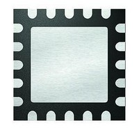
PIC16F1507-I/ML Microchip Technology, PIC16F1507-I/ML Datasheet - Page 15

PIC16F1507-I/ML
Manufacturer Part Number
PIC16F1507-I/ML
Description
3.5KB Flash, 128B RAM, 18 I/O, CLC, CWG, DDS, 10-bit ADC 20 QFN 4x4mm TUBE
Manufacturer
Microchip Technology
Series
PIC® 16Fr
Datasheets
1.PIC16F1507-EML.pdf
(266 pages)
2.PIC16F1507-EML.pdf
(26 pages)
3.PIC16F1507-EML.pdf
(40 pages)
Specifications of PIC16F1507-I/ML
Processor Series
PIC16
Core
PIC16F
Data Bus Width
8 bit
Program Memory Type
Flash
Program Memory Size
3.5 KB
Data Ram Size
128 B
Interface Type
ICSP
Maximum Clock Frequency
20 MHz
Number Of Programmable I/os
18
Number Of Timers
3
Operating Supply Voltage
2.3 V to 5.5 V
Maximum Operating Temperature
+ 85 C
Mounting Style
SMD/SMT
Package / Case
QFN-20
Minimum Operating Temperature
- 40 C
Operating Temperature Range
- 40 C to + 85 C
Supply Current (max)
30 uA
Core Processor
PIC
Core Size
8-Bit
Speed
20MHz
Connectivity
-
Peripherals
Brown-out Detect/Reset, POR, PWM, WDT
Number Of I /o
17
Eeprom Size
-
Ram Size
128 x 8
Voltage - Supply (vcc/vdd)
2.3 V ~ 5.5 V
Data Converters
A/D 12x10b
Oscillator Type
Internal
Operating Temperature
-40°C ~ 85°C
Lead Free Status / Rohs Status
Details
Available stocks
Company
Part Number
Manufacturer
Quantity
Price
Part Number:
PIC16F1507-I/ML
Manufacturer:
MICROCHIP/微芯
Quantity:
20 000
4.3
The devices implement 10 programming commands;
each six bits in length. The commands are summarized
in
Commands that have data associated with them are
specified to have a minimum delay of T
command and the data. After this delay 16 clocks are
required to either clock in or clock out the 14-bit data
word. The first clock is for the Start bit and the last clock
is for the Stop bit.
TABLE 4-1:
4.3.1
The Load Configuration command is used to access
the
Configuration Words, Calibration Words). The Load
Configuration command sets the address to 8000h and
loads the data latches with one word of data (see
Figure
After issuing the Load Configuration command, use the
Increment Address command until the proper address
to be programmed is reached. The address is then pro-
grammed by issuing either the Begin Internally Timed
Programming or Begin Externally Timed Programming
command.
FIGURE 4-1:
2011 Microchip Technology Inc.
Load Configuration
Load Data For Program Memory
Read Data From Program Memory
Increment Address
Reset Address
Begin Internally Timed Programming
Begin Externally Timed Programming
End Externally Timed Programming
Bulk Erase Program Memory
Row Erase Program Memory
Table
configuration
4-1).
ICSPDAT
ICSPCLK
4-1.
Program/Verify Commands
LOAD CONFIGURATION
Command
COMMAND MAPPING
memory
LOAD CONFIGURATION
1
0
2
(user
0
3
DLY
0
PIC12(L)F1501/PIC16(L)F150X
ID
x
x
x
x
x
x
x
x
x
x
between the
Advance Information
4
0
locations,
Binary (MSb … LSb)
0
0
0
0
1
0
1
0
0
1
5
0
0
0
0
0
0
1
1
1
1
0
6
X
Mapping
0
0
1
1
1
0
0
0
0
0
T
DLY
The only way to get back to the program memory
(address 0) is to exit Program/Verify mode or issue the
Reset Address command after the configuration memory
has been accessed by the Load Configuration command.
Note:
0
1
0
1
1
0
0
1
0
0
1
0
0
0
0
0
0
0
0
0
1
1
Externally timed writes are not supported
for Configuration and Calibration bits. Any
externally timed write to the Configuration
or Calibration Word will have no effect on
the targeted word.
2
LSb
Hex
0Ah
00h
02h
04h
06h
16h
08h
18h
09h
11h
0, data (14), 0
0, data (14), 0
0, data (14), 0
—
—
—
—
—
Internally Timed
Internally Timed
15
MSb 0
Data/Note
16
DS41573C-page 15


