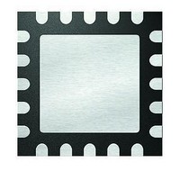
PIC16F1507-I/ML Microchip Technology, PIC16F1507-I/ML Datasheet - Page 29

PIC16F1507-I/ML
Manufacturer Part Number
PIC16F1507-I/ML
Description
3.5KB Flash, 128B RAM, 18 I/O, CLC, CWG, DDS, 10-bit ADC 20 QFN 4x4mm TUBE
Manufacturer
Microchip Technology
Series
PIC® 16Fr
Datasheets
1.PIC16F1507-EML.pdf
(266 pages)
2.PIC16F1507-EML.pdf
(26 pages)
3.PIC16F1507-EML.pdf
(40 pages)
Specifications of PIC16F1507-I/ML
Processor Series
PIC16
Core
PIC16F
Data Bus Width
8 bit
Program Memory Type
Flash
Program Memory Size
3.5 KB
Data Ram Size
128 B
Interface Type
ICSP
Maximum Clock Frequency
20 MHz
Number Of Programmable I/os
18
Number Of Timers
3
Operating Supply Voltage
2.3 V to 5.5 V
Maximum Operating Temperature
+ 85 C
Mounting Style
SMD/SMT
Package / Case
QFN-20
Minimum Operating Temperature
- 40 C
Operating Temperature Range
- 40 C to + 85 C
Supply Current (max)
30 uA
Core Processor
PIC
Core Size
8-Bit
Speed
20MHz
Connectivity
-
Peripherals
Brown-out Detect/Reset, POR, PWM, WDT
Number Of I /o
17
Eeprom Size
-
Ram Size
128 x 8
Voltage - Supply (vcc/vdd)
2.3 V ~ 5.5 V
Data Converters
A/D 12x10b
Oscillator Type
Internal
Operating Temperature
-40°C ~ 85°C
Lead Free Status / Rohs Status
Details
Available stocks
Company
Part Number
Manufacturer
Quantity
Price
Part Number:
PIC16F1507-I/ML
Manufacturer:
MICROCHIP/微芯
Quantity:
20 000
7.3
The checksum is calculated by two different methods
dependent on the setting of the CP Configuration bit.
TABLE 7-1:
EXAMPLE 7-1:
2011 Microchip Technology Inc.
PIC12(L)F1501
PIC16(L)F1503
PIC16(L)F1507
PIC16(L)F1508
PIC16(L)F1509
Note 1:
PIC16F1507
Device
2:
3:
4:
5:
6:
Checksum Computation
This value is obtained by taking the total number of program memory locations (0x000 to 0x7FFh which
is 800h) and multiplying it by the blank memory value of 0x3FFF to get the sum of 1FF F800h. Then,
truncate to 16 bits, thus having a final value of F800h.
This value is obtained by making all bits of the Configuration Word 1 a ‘1’, then converting it to hex, thus
having a value of 3FFFh.
This value is obtained by making all used bits of the Configuration Word 1 a ‘1’, then converting it to hex,
thus having a value of 0EFBh.
This value is obtained by making all bits of the Configuration Word 2 a ‘1’, then converting it to hex, thus
having a value of 3FFFh.
This value is obtained by making all used bits of the Configuration Word 2 a ‘1’, then converting it to hex,
thus having a value of 2E03h.
This value is obtained by ANDing the Configuration Word value with the Configuration Word Mask Value
and adding it to the sum of memory addresses: (3FFFh and 0EFBh) + (3FFFh and 2E03h) + F800h =
1 34FEh. Then, truncate to 16 bits, thus having a final value of 34FEh.
CONFIGURATION WORD
MASK VALUES
Sum of Memory addresses 0000h-07FFh
Configuration Word 1
Configuration Word 1 mask
Configuration Word 2
Configuration Word 2 mask
Checksum
CHECKSUM COMPUTED WITH PROGRAM CODE PROTECTION DISABLED
(CP = 1), PIC16F1507, BLANK DEVICE
Config. Word
1 Mask
0EFBh
0EFBh
0EFBh
3EFFh
3EFFh
PIC12(L)F1501/PIC16(L)F150X
Config. Word
= F800h + (3FFFh and 0EFBh) + (3FFFh and 2E03h)
= F800h + 0EFBh + 2E03h
= 34FEh
2 Mask
2E03h
2E03h
2E03h
3E03h
3E03h
Advance Information
7.3.1
With the program code protection disabled, the
checksum is computed by reading the contents of the
program memory locations and adding up the program
memory data starting at address 0000h, up to the
maximum user addressable location. Any Carry bit
exceeding 16 bits are ignored. Additionally, the relevant
bits of the Configuration Words are added to the
checksum. All unimplemented Configuration bits are
masked to ‘0’.
F800h
3FFFh
0EFBh
3FFFh
2E03h
PROGRAM CODE PROTECTION
DISABLED
(1)
(5)
(2)
(4)
(3)
(6)
DS41573C-page 29


