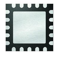
PIC16F1507-I/ML Microchip Technology, PIC16F1507-I/ML Datasheet - Page 14

PIC16F1507-I/ML
Manufacturer Part Number
PIC16F1507-I/ML
Description
3.5KB Flash, 128B RAM, 18 I/O, CLC, CWG, DDS, 10-bit ADC 20 QFN 4x4mm TUBE
Manufacturer
Microchip Technology
Series
PIC® 16Fr
Datasheets
1.PIC16F1507-EML.pdf
(266 pages)
2.PIC16F1507-EML.pdf
(26 pages)
3.PIC16F1507-EML.pdf
(40 pages)
Specifications of PIC16F1507-I/ML
Processor Series
PIC16
Core
PIC16F
Data Bus Width
8 bit
Program Memory Type
Flash
Program Memory Size
3.5 KB
Data Ram Size
128 B
Interface Type
ICSP
Maximum Clock Frequency
20 MHz
Number Of Programmable I/os
18
Number Of Timers
3
Operating Supply Voltage
2.3 V to 5.5 V
Maximum Operating Temperature
+ 85 C
Mounting Style
SMD/SMT
Package / Case
QFN-20
Minimum Operating Temperature
- 40 C
Operating Temperature Range
- 40 C to + 85 C
Supply Current (max)
30 uA
Core Processor
PIC
Core Size
8-Bit
Speed
20MHz
Connectivity
-
Peripherals
Brown-out Detect/Reset, POR, PWM, WDT
Number Of I /o
17
Eeprom Size
-
Ram Size
128 x 8
Voltage - Supply (vcc/vdd)
2.3 V ~ 5.5 V
Data Converters
A/D 12x10b
Oscillator Type
Internal
Operating Temperature
-40°C ~ 85°C
Lead Free Status / Rohs Status
Details
Available stocks
Company
Part Number
Manufacturer
Quantity
Price
Part Number:
PIC16F1507-I/ML
Manufacturer:
MICROCHIP/微芯
Quantity:
20 000
PIC12(L)F1501/PIC16(L)F150X
4.0
In Program/Verify mode, the program memory and the
configuration
programmed
ICSPCLK are used for the data and the clock,
respectively. All commands and data words are
transmitted LSb first. Data changes on the rising edge
of the ICSPCLK and latched on the falling edge. In
Program/Verify
ICSPCLK are Schmitt Trigger inputs. The sequence
that enters the device into Program/Verify mode
places all other logic into the Reset state. Upon
entering
automatically configured as high-impedance inputs
and the address is cleared.
4.1
There are two different methods of entering Program/
Verify mode via high-voltage:
• V
• V
4.1.1
To enter Program/Verify mode via the V
the following sequence must be followed:
1.
2.
3.
The V
code prior to entering Program/Verify mode. For
example, the device will execute code when
Configuration Word 1 has MCLR disabled (MCLRE =
0), the Power-up Timer is disabled (PWRTE = 0), the
internal oscillator is selected (F
ICSPCLK and ICSPDAT pins are driven by the user
application. Since this may prevent entry, V
entry mode is strongly recommended. See the timing
diagram in
4.1.2
To enter Program/Verify mode via the V
the following sequence must be followed:
1.
2.
3.
The V
device when V
necessary to disconnect V
mode. See the timing diagram in
DS41573C-page 14
PP
DD
Hold ICSPCLK and ICSPDAT low. All other pins
should be unpowered.
Raise the voltage on MCLR from 0V to V
Raise the voltage on V
operating voltage.
Hold ICSPCLK and ICSPDAT low.
Raise the voltage on V
operating voltage.
Raise the voltage on MCLR from V
to V
PP
DD
– First entry mode
– First entry mode
-first entry prevents the device from executing
IHH
-first method is useful when programming the
PROGRAM/VERIFY MODE
High-Voltage Program/Verify Mode
Entry and Exit
Program/Verify
Figure
.
V
V
PP
DD
in
memory
DD
– FIRST ENTRY MODE
– FIRST ENTRY MODE
mode
8-2.
serial
is already applied, for it is not
both
can
DD
DD
DD
fashion.
mode,
from 0V to the desired
from 0V to the desired
to enter Program/Verify
the
be
Figure
OSC
accessed
ICSPDAT
ICSPDAT
all
DD
PP
DD
8-1.
= 100), and
-first method
-first method
or below
Advance Information
I/Os
IHH
PP
.
-first
and
and
and
are
4.1.3
To exit Program/Verify mode take MCLR to V
lower (V
4.2
The Low-Voltage Programming mode allows devices to
be programmed using V
When the LVP bit of Configuration Word 2 register is
set to ‘1’, the low-voltage ICSP programming entry is
enabled. To disable the Low-Voltage ICSP mode, the
LVP bit must be programmed to ‘0’. This can only be
done while in the High-Voltage Entry mode.
Entry into the Low-Voltage ICSP Program/Verify modes
requires the following steps:
1.
2.
The key sequence is a specific 32-bit pattern, '0100
1101 0100 0011 0100 1000 0101 0000' (more
easily remembered as MCHP in ASCII). The device will
enter Program/Verify mode only if the sequence is
valid. The Least Significant bit of the Least Significant
nibble must be shifted in first.
Once the key sequence is complete, MCLR must be
held at V
maintained.
For low-voltage programming timing, see
and
Exiting Program/Verify mode is done by no longer
driving MCLR to V
Note:
MCLR is brought to V
A 32-bit key sequence is presented on
ICSPDAT, while clocking ICSPCLK.
Figure
IL
IL
Low-Voltage Programming (LVP)
Mode
). See Figures
for as long as Program/Verify mode is to be
8-9.
PROGRAM/VERIFY MODE EXIT
To enter LVP mode, the LSB of the Least
Significant nibble must be shifted in first.
This differs from entering the key
sequence on other parts.
IL
. See
2011 Microchip Technology Inc.
8-3
DD
Figure 8-8
IL
.
only, without high voltage.
and 8-4.
and
Figure
Figure 8-8
8-9.
DD
or


