PIC24FJ16MC102-I/SO Microchip Technology, PIC24FJ16MC102-I/SO Datasheet - Page 183
PIC24FJ16MC102-I/SO
Manufacturer Part Number
PIC24FJ16MC102-I/SO
Description
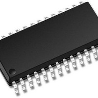
16-bit Motor Control Family, 16 MIPS, 16KB Flash, 1KB RAM 28 SOIC .300in TUBE
Manufacturer
Microchip Technology
Series
PIC® 24Fr
Datasheet
1.PIC24FJ16MC101-IP.pdf
(304 pages)
Specifications of PIC24FJ16MC102-I/SO
Processor Series
PIC24FJ
Core
PIC
Data Bus Width
16 bit
Program Memory Type
Flash
Program Memory Size
16 KB
Data Ram Size
1 KB
Maximum Operating Temperature
+ 85 C
Mounting Style
SMD/SMT
Package / Case
SOIC-28
Development Tools By Supplier
MPLAB IDE Software
Minimum Operating Temperature
- 40 C
Featured Product
PIC24FJ/33FJ MCUs & dsPIC® DSCs
Core Processor
PIC
Core Size
16-Bit
Speed
16 MIPs
Connectivity
I²C, IrDA, LIN, SPI, UART/USART
Peripherals
Brown-out Detect/Reset, Motor Control PWM, POR, PWM, WDT
Number Of I /o
21
Eeprom Size
-
Ram Size
1K x 8
Voltage - Supply (vcc/vdd)
3 V ~ 3.6 V
Data Converters
A/D 6x10b
Oscillator Type
Internal
Operating Temperature
-40°C ~ 85°C
Lead Free Status / Rohs Status
Details


REGISTER 19-6:
© 2011 Microchip Technology Inc.
,2
bit 15
bit 7
Legend:
R = Readable bit
-n = Value at POR
bit 15-6
bit 5-0
Note 1:
U-0
U-0
—
—
2:
3:
On devices without 6 analog inputs, all AD1CSSL bits can be selected by user application. However,
inputs selected for scan without a corresponding input on device converts V
CSSx = ANx, where x = 0 through 5.
CTMU temperature sensor input cannot be scanned.
Unimplemented: Read as ‘0’
CSS<5:0>: ADC Input Scan Selection bits
1 = Select ANx for input scan
0 = Skip ANx for input scan
U-0
U-0
—
—
AD1CSSL: ADC1 INPUT SCAN SELECT REGISTER LOW
‘1’ = Bit is set
W = Writable bit
R/W-0
CSS5
U-0
—
R/W-0
CSS4
Preliminary
U-0
—
U = Unimplemented bit, read as ‘0’
‘0’ = Bit is cleared
R/W-0
CSS3
U-0
—
PIC24FJ16MC101/102
R/W-0
CSS2
U-0
—
REFL
(1,2,3)
x = Bit is unknown
.
R/W-0
CSS1
U-0
—
DS39997B-page 183
R/W-0
CSS0
U-0
—
bit 8
bit 0
Related parts for PIC24FJ16MC102-I/SO
Image
Part Number
Description
Manufacturer
Datasheet
Request
R

Part Number:
Description:
Manufacturer:
Microchip Technology Inc.
Datasheet:
Part Number:
Description:
Manufacturer:
Microchip Technology Inc.
Datasheet:
Part Number:
Description:
Manufacturer:
Microchip Technology Inc.
Datasheet:
Part Number:
Description:
Manufacturer:
Microchip Technology Inc.
Datasheet:
Part Number:
Description:
Manufacturer:
Microchip Technology Inc.
Datasheet:
Part Number:
Description:
Manufacturer:
Microchip Technology Inc.
Datasheet:
Part Number:
Description:
Manufacturer:
Microchip Technology Inc.
Datasheet:
Part Number:
Description:
Manufacturer:
Microchip Technology Inc.
Datasheet: