PIC24FJ16MC102-I/SO Microchip Technology, PIC24FJ16MC102-I/SO Datasheet - Page 184
PIC24FJ16MC102-I/SO
Manufacturer Part Number
PIC24FJ16MC102-I/SO
Description
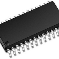
16-bit Motor Control Family, 16 MIPS, 16KB Flash, 1KB RAM 28 SOIC .300in TUBE
Manufacturer
Microchip Technology
Series
PIC® 24Fr
Datasheet
1.PIC24FJ16MC101-IP.pdf
(304 pages)
Specifications of PIC24FJ16MC102-I/SO
Processor Series
PIC24FJ
Core
PIC
Data Bus Width
16 bit
Program Memory Type
Flash
Program Memory Size
16 KB
Data Ram Size
1 KB
Maximum Operating Temperature
+ 85 C
Mounting Style
SMD/SMT
Package / Case
SOIC-28
Development Tools By Supplier
MPLAB IDE Software
Minimum Operating Temperature
- 40 C
Featured Product
PIC24FJ/33FJ MCUs & dsPIC® DSCs
Core Processor
PIC
Core Size
16-Bit
Speed
16 MIPs
Connectivity
I²C, IrDA, LIN, SPI, UART/USART
Peripherals
Brown-out Detect/Reset, Motor Control PWM, POR, PWM, WDT
Number Of I /o
21
Eeprom Size
-
Ram Size
1K x 8
Voltage - Supply (vcc/vdd)
3 V ~ 3.6 V
Data Converters
A/D 6x10b
Oscillator Type
Internal
Operating Temperature
-40°C ~ 85°C
Lead Free Status / Rohs Status
Details


PIC24FJ16MC101/102
REGISTER 19-7:
DS39997B-page 184
bit 15
bit 7
Legend:
R = Readable bit
-n = Value at POR
bit 15-6
bit 5-0
Note 1:
U-0
U-0
—
—
2:
3:
4:
On devices without 6 analog inputs, all PCFG bits are R/W by user. However, PCFG bits are ignored on
ports without a corresponding input on device.
PCFGx = ANx, where x = 0 through 5.
PCFGx bits have no effect if the ADC module is disabled by setting ADxMD bit in the PMDx register. When
the bit is set, all port pins that have been multiplexed with ANx will be in Digital mode.
Pins shared with analog functions (i.e., ANx), are analog by default and therefore, must be set by the user
to enable any digital function on that pin. Reading any port pin with the analog function enabled will return
a ‘0’, regardless of the signal input level.
Unimplemented: Read as ‘0’
PCFG<5:0>: ADC Port Configuration Control bits
1 = Port pin in Digital mode, port read input enabled, ADC input multiplexer connected to AV
0 = Port pin in Analog mode, port read input disabled, ADC samples pin voltage
U-0
U-0
—
—
AD1PCFGL: ADC1 PORT CONFIGURATION REGISTER LOW
W = Writable bit
‘1’ = Bit is set
PCFG5
R/W-0
U-0
—
(4)
PCFG4
R/W-0
Preliminary
U-0
—
(4)
U = Unimplemented bit, read as ‘0’
‘0’ = Bit is cleared
PCFG3
R/W-0
U-0
—
(4)
(4)
PCFG2
R/W-0
U-0
—
(4)
© 2011 Microchip Technology Inc.
x = Bit is unknown
PCFG1
R/W-0
(1,2,3)
U-0
—
(4)
PCFG0
R/W-0
SS
U-0
—
bit 8
bit 0
(4)
Related parts for PIC24FJ16MC102-I/SO
Image
Part Number
Description
Manufacturer
Datasheet
Request
R

Part Number:
Description:
Manufacturer:
Microchip Technology Inc.
Datasheet:
Part Number:
Description:
Manufacturer:
Microchip Technology Inc.
Datasheet:
Part Number:
Description:
Manufacturer:
Microchip Technology Inc.
Datasheet:
Part Number:
Description:
Manufacturer:
Microchip Technology Inc.
Datasheet:
Part Number:
Description:
Manufacturer:
Microchip Technology Inc.
Datasheet:
Part Number:
Description:
Manufacturer:
Microchip Technology Inc.
Datasheet:
Part Number:
Description:
Manufacturer:
Microchip Technology Inc.
Datasheet:
Part Number:
Description:
Manufacturer:
Microchip Technology Inc.
Datasheet: