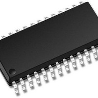
PIC24FJ16MC102-I/SO Microchip Technology, PIC24FJ16MC102-I/SO Datasheet - Page 44

PIC24FJ16MC102-I/SO
Manufacturer Part Number
PIC24FJ16MC102-I/SO
Description
16-bit Motor Control Family, 16 MIPS, 16KB Flash, 1KB RAM 28 SOIC .300in TUBE
Manufacturer
Microchip Technology
Series
PIC® 24Fr
Datasheet
1.PIC24FJ16MC101-IP.pdf
(304 pages)
Specifications of PIC24FJ16MC102-I/SO
Processor Series
PIC24FJ
Core
PIC
Data Bus Width
16 bit
Program Memory Type
Flash
Program Memory Size
16 KB
Data Ram Size
1 KB
Maximum Operating Temperature
+ 85 C
Mounting Style
SMD/SMT
Package / Case
SOIC-28
Development Tools By Supplier
MPLAB IDE Software
Minimum Operating Temperature
- 40 C
Featured Product
PIC24FJ/33FJ MCUs & dsPIC® DSCs
Core Processor
PIC
Core Size
16-Bit
Speed
16 MIPs
Connectivity
I²C, IrDA, LIN, SPI, UART/USART
Peripherals
Brown-out Detect/Reset, Motor Control PWM, POR, PWM, WDT
Number Of I /o
21
Eeprom Size
-
Ram Size
1K x 8
Voltage - Supply (vcc/vdd)
3 V ~ 3.6 V
Data Converters
A/D 6x10b
Oscillator Type
Internal
Operating Temperature
-40°C ~ 85°C
Lead Free Status / Rohs Status
Details
- Current page: 44 of 304
- Download datasheet (5Mb)
PIC24FJ16MC101/102
4.2.5
In addition to its use as a working register, the W15
register in the PIC24FJ16MC101/102 devices is also
used as a software Stack Pointer. The Stack Pointer
always points to the first available free word and grows
from lower to higher addresses. It pre-decrements for
stack pops and post-increments for stack pushes, as
shown in
instruction, the MSb of the PC is zero-extended before
the push, ensuring that the MSb is always clear.
The Stack Pointer Limit register (SPLIM) associated
with the Stack Pointer sets an upper address boundary
for the stack. SPLIM is uninitialized at Reset. As is the
case for the Stack Pointer, SPLIM<0> is forced to ‘0’
because all stack operations must be word aligned.
Whenever an EA is generated using W15 as a source
or destination pointer, the resulting address is
compared with the value in SPLIM. If the contents of
the Stack Pointer (W15) and the SPLIM register are
equal and a push operation is performed, a stack error
trap will not occur. However, the stack error trap will
occur on a subsequent push operation. For example, to
cause a stack error trap when the stack grows beyond
address 0x0C00 in RAM, initialize the SPLIM with the
value 0x0BFE.
Similarly, a Stack Pointer underflow (stack error) trap is
generated when the Stack Pointer address is found to
be less than 0x0800. This prevents the stack from
interfering with the SFR space.
A write to the SPLIM register should not be immediately
followed by an indirect read operation using W15.
FIGURE 4-4:
DS39997B-page 44
0x0000
Note:
Figure
15
000000000
SOFTWARE STACK
A PC push during exception processing
concatenates the SRL register to the MSb
of the PC prior to the push.
<Free Word>
PC<15:0>
4-4. For a PC push during any CALL
PC<22:16>
CALL STACK FRAME
0
POP : [--W15]
PUSH : [W15++]
W15 (before CALL)
W15 (after CALL)
Preliminary
4.2.6
The PIC24FXXXX product family supports Data RAM
protection features that enable segments of RAM to be
protected when used in conjunction with Boot and
Secure Code Segment Security. BSRAM (Secure RAM
segment for BS) is accessible only from the Boot
Segment Flash code, when enabled. SSRAM (Secure
RAM segment for RAM) is accessible only from the
Secure Segment Flash code, when enabled. See
Table 4-1
SFRs.
4.3
The addressing modes shown in
basis of the addressing modes that are optimized to
support the specific features of individual instructions.
The addressing modes provided in the MAC class of
instructions differ from those provided in other
instruction types.
4.3.1
Most file register instructions use a 13-bit address field
(f) to directly address data present in the first 8192
bytes of data memory (near data space). Most file
register instructions employ a working register, W0,
which is denoted as WREG in these instructions. The
destination is typically either the same file register or
WREG (with the exception of the MUL instruction),
which writes the result to a register or register pair. The
MOV instruction allows additional flexibility and can
access the entire data space.
4.3.2
The three-operand MCU instructions are of the form:
Operand 3 = Operand 1 <function> Operand 2
where Operand 1 is always a working register (that is,
the addressing mode can only be register direct), which
is referred to as Wb. Operand 2 can be a W register,
fetched from data memory, or a 5-bit literal. The result
location can be either a W register or a data memory
location.
supported by MCU instructions:
• Register Direct
• Register Indirect
• Register Indirect Post-Modified
• Register Indirect Pre-Modified
• 5-bit or 10-bit Literal
Note:
Instruction Addressing Modes
for an overview of the BSRAM and SSRAM
The
DATA RAM PROTECTION FEATURE
FILE REGISTER INSTRUCTIONS
MCU INSTRUCTIONS
Not all instructions support all of the
addressing
Individual
different subsets of these addressing
modes.
following
© 2011 Microchip Technology Inc.
instructions
modes
addressing
Table 4-27
given
can
modes
form the
support
above.
are
Related parts for PIC24FJ16MC102-I/SO
Image
Part Number
Description
Manufacturer
Datasheet
Request
R

Part Number:
Description:
Manufacturer:
Microchip Technology Inc.
Datasheet:

Part Number:
Description:
Manufacturer:
Microchip Technology Inc.
Datasheet:

Part Number:
Description:
Manufacturer:
Microchip Technology Inc.
Datasheet:

Part Number:
Description:
Manufacturer:
Microchip Technology Inc.
Datasheet:

Part Number:
Description:
Manufacturer:
Microchip Technology Inc.
Datasheet:

Part Number:
Description:
Manufacturer:
Microchip Technology Inc.
Datasheet:

Part Number:
Description:
Manufacturer:
Microchip Technology Inc.
Datasheet:

Part Number:
Description:
Manufacturer:
Microchip Technology Inc.
Datasheet:


