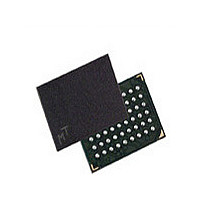
MT48H4M16LFB4-75 IT:H Micron Technology Inc, MT48H4M16LFB4-75 IT:H Datasheet - Page 25

MT48H4M16LFB4-75 IT:H
Manufacturer Part Number
MT48H4M16LFB4-75 IT:H
Description
Manufacturer
Micron Technology Inc
Type
SDRAMr
Datasheet
1.MT48H4M16LFB4-75_ITH.pdf
(62 pages)
Specifications of MT48H4M16LFB4-75 IT:H
Organization
4Mx16
Density
64Mb
Address Bus
14b
Maximum Clock Rate
133MHz
Operating Supply Voltage (typ)
1.8V
Package Type
VFBGA
Operating Temp Range
-40C to 85C
Operating Supply Voltage (max)
1.9V
Operating Supply Voltage (min)
1.7V
Supply Current
50mA
Pin Count
54
Mounting
Surface Mount
Operating Temperature Classification
Industrial
Lead Free Status / RoHS Status
Compliant
Figure 17:
Figure 18:
PDF: 09005aef8237ed98/Source: 09005aef8237ed68
64mb_x16_Mobile SDRAM_Y24L_2.fm - Rev. C 10/07 EN
WRITE Burst
WRITE-to-WRITE
Note:
Note:
WRITE command. Full-speed random write accesses within a page can be performed to
the same bank, as shown in Figure 19 on page 26, or each subsequent WRITE may be
performed to a different bank.
Command
Command
Data for any WRITE burst may be truncated with a subsequent READ command, and
data for a fixed-length WRITE burst may be immediately followed by a READ command.
After the READ command is registered, the data inputs will be ignored and writes will
not be executed. An example is shown in Figure 20 on page 26. Data n + 1 is either the
last of a burst of two or the last desired of a longer burst.
Data for a fixed-length WRITE burst may be followed by, or truncated with, a
PRECHARGE command to the same bank (provided that auto precharge was not acti-
vated). The PRECHARGE command should be issued
the last desired input data element is registered. The auto precharge mode requires a
t
In addition, when truncating a WRITE burst, the DQM signal must be used to mask
input data for the clock edge prior to, and the clock edge coincident with, the
PRECHARGE command. An example is shown in Figure 21 on page 27. Data n + 1 is
WR of at least one clock plus time, regardless of frequency.
Address
Address
BL = 2. DQM is LOW.
DQM is LOW. Each WRITE command may be issued to any bank.
CLK
CLK
Transitioning Data
DQ
DQ
WRITE
Bank,
Col n
WRITE
Bank,
Transitioning Data
T0
Col n
D
D
T0
n
n
IN
IN
NOP
n + 1
T1
n + 1
NOP
D
T1
D
IN
IN
Don’t Care
25
WRITE
NOP
Bank,
Col b
T2
T2
D
b
IN
Don’t Care
Micron Technology, Inc., reserves the right to change products or specifications without notice.
T3
NOP
64Mb: 4 Meg x 16 Mobile SDRAM
t
WR after the clock edge at which
©2006 Micron Technology, Inc. All rights reserved.
Operations


