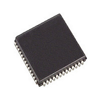
IDT7130SA55JG IDT, Integrated Device Technology Inc, IDT7130SA55JG Datasheet - Page 9

IDT7130SA55JG
Manufacturer Part Number
IDT7130SA55JG
Description
Manufacturer
IDT, Integrated Device Technology Inc
Datasheet
1.IDT7130SA55JG.pdf
(19 pages)
Specifications of IDT7130SA55JG
Density
8Kb
Access Time (max)
55ns
Sync/async
Asynchronous
Architecture
Not Required
Clock Freq (max)
Not RequiredMHz
Operating Supply Voltage (typ)
5V
Address Bus
20b
Package Type
PLCC
Operating Temp Range
0C to 70C
Number Of Ports
2
Supply Current
155mA
Operating Supply Voltage (min)
4.5V
Operating Supply Voltage (max)
5.5V
Operating Temperature Classification
Commercial
Mounting
Surface Mount
Pin Count
52
Word Size
8b
Number Of Words
1K
Lead Free Status / RoHS Status
Compliant
Timing Waveform of Read Cycle No. 1, Either Side
NOTES:
1. R/W = V
2. t
3. Start of valid data depends on which timing becomes effective last t
Timing Waveform of Read Cycle No. 2, Either Side
CURRENT
NOTES:
1. Timing depends on which signal is asserted last, OE or CE.
2. Timing depends on which signal is deaserted first, OE or CE.
3. R/W = V
4. Start of valid data depends on which timing becomes effective last t
ADDRESS
DATA
BUSY
DATA
IDT7130SA/LA and IDT7140SA/LA
High-Speed 1K x 8 Dual-Port Static SRAM
BUSY has no relationship to valid output data.
BDD
delay is required only in the case where the opposite port is completing a write operation to the same the address location. For simultaneous read operations,
OUT
OUT
OUT
I
CE
OE
I
CC
SS
IH
IH
, CE = V
and OE = V
PREVIOUS DATA VALID
IL
, and is OE = V
IL
, and the address is valid prior to or coincidental with CE transition LOW.
IL
. Address is valid prior to the coincidental with CE transition LOW.
t
OH
t
t
AA
PU
50%
t
LZ
t
(1)
t
ACE
RC
AOE
AOE
t
, t
, t
BDDH
t
LZ
ACE
ACE
t
AOE
(1)
, t
,
t
AA
AA
(2,3)
, and t
(4)
, and
9
t
BDD
BDD
DATA VALID
.
.
Military, Industrial and Commercial Temperature Ranges
VALID DATA
t
(1)
(3)
OH
t
t
PD
HZ
(4)
(2)
t
HZ
50%
(2)
2689 drw 08
2689 drw 09


