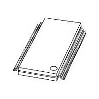
SSTV16857DGG NXP Semiconductors, SSTV16857DGG Datasheet - Page 4

SSTV16857DGG
Manufacturer Part Number
SSTV16857DGG
Description
Manufacturer
NXP Semiconductors
Datasheet
1.SSTV16857DGG.pdf
(12 pages)
Specifications of SSTV16857DGG
Logic Family
SSTV
Logical Function
Registered Buffer
Number Of Elements
1
Number Of Bits
14
Number Of Inputs
14
Number Of Outputs
14
High Level Output Current
-20mA
Low Level Output Current
20mA
Propagation Delay Time
2.4ns
Operating Supply Voltage (typ)
2.5V
Operating Supply Voltage (max)
2.7V
Operating Supply Voltage (min)
2.3V
Clock-edge Trigger Type
Posit/Negat-Edge
Polarity
Non-Inverting
Technology
CMOS
Frequency (max)
200MHz
Mounting
Surface Mount
Pin Count
48
Operating Temp Range
0C to 70C
Operating Temperature Classification
Commercial
Lead Free Status / RoHS Status
Compliant
1. Stresses beyond those listed may cause permanent damage to the device. These are stress ratings only and functional operation of the
2. The performance capability of a high-performance integrated circuit in conjunction with its thermal environment can create junction
3. The input and output voltage ratings may be exceeded if the input and output current ratings are observed.
4. The continuous current at V
Philips Semiconductors
BALL CONFIGURATION
ABSOLUTE MAXIMUM RATINGS
NOTES:
2002 Sep 27
SYMBOL
SYMBOL
14-bit SSTL_2 registered driver
with differential clock inputs
device at these or any other conditions beyond those indicated under “recommended operating conditions” is not implied. Exposure to
absolute-maximum-rated conditions for extended periods may affect device reliability.
temperatures which are detrimental to reliability. The maximum junction temperature of this integrated circuit should not exceed 150 C.
V
I
I
V
T
I
O
OUT
I
OK
OUT
V
stg
CC
IK
I
Storage temperature range
DC output diode current
DC input diode current
Continuous current
DC output voltage
DC supply voltage
DC input voltage
DC output current
PARAMETER
PARAMETER
C
D
G
H
A
B
E
F
J
K
CC
, V
DDQ
GND
GND
GND
V
V
V
Q11
Q14
Q1
Q4
1
CC
CC
CC
3
3
, or GND should not exceed 100 mA.
4
1
2
GND
GND
Q12
Q13
NC
Q2
Q3
Q7
Q8
NC
2
Q10
V
V
NC
NC
Q5
Q6
Q9
CC
CC
3
V
CC
4
V
CONDITION
CONDITION
O
, V
= 0 to V
V
V
DDQ
RESET
O
CLK–
I
V
D10
V
NC
NC
D5
4
CC
CC
< 0
< 0
, or GND
DDQ
CLK+
V
D12
D13
5
NC
NC
D2
D3
D6
D9
REF
6
GND
GND
GND
V
D11
D14
D1
D4
D7
D8
CC
–0.5
–0.5
–0.5
MIN
–65
—
—
—
—
LIMITS
SW00952
SSTV16857
V
V
DDQ
DDQ
MAX
+150
+4.6
–50
–50
100
50
+ 0.5
+ 0.5
Product data
UNIT
UNIT
mA
mA
mA
mA
V
V
V
C


