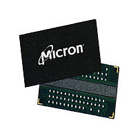
MT47H128M16HG-37E:A Micron Technology Inc, MT47H128M16HG-37E:A Datasheet - Page 41

MT47H128M16HG-37E:A
Manufacturer Part Number
MT47H128M16HG-37E:A
Description
Manufacturer
Micron Technology Inc
Type
DDR2 SDRAMr
Datasheet
1.MT47H128M16HG-37EA.pdf
(134 pages)
Specifications of MT47H128M16HG-37E:A
Organization
128Mx16
Address Bus
17b
Access Time (max)
500ps
Maximum Clock Rate
533MHz
Operating Supply Voltage (typ)
1.8V
Package Type
FBGA
Operating Temp Range
0C to 70C
Operating Supply Voltage (max)
1.9V
Operating Supply Voltage (min)
1.7V
Supply Current
195mA
Pin Count
84
Mounting
Surface Mount
Operating Temperature Classification
Commercial
Lead Free Status / RoHS Status
Compliant
18. The inputs to the DRAM must be aligned to the associated clock, that is, the actual clock that latches it in. Howev-
19. The DRAM output timing is aligned to the nominal or average clock. Most output parameters must be derated by
20. When DQS is used single-ended, the minimum limit is reduced by 100ps.
21.
22.
23. This is not a device limit. The device will operate with a negative value, but system performance could be degra-
24. It is recommended that DQS be valid (HIGH or LOW) on or before the WRITE command. The case shown (DQS
25. The intent of the “Don’t Care” state after completion of the postamble is that the DQS-driven signal should either
26. Referenced to each output group: x4 = DQS with DQ0–DQ3; x8 = DQS with DQ0–DQ7; x16 = LDQS with DQ0–DQ7;
27. The data valid window is derived by achieving other specifications:
28.
29. This maximum value is derived from the referenced test load.
30. The values listed are for the differential DQS strobe (DQS and DQS#) with a differential slew rate of 2 V/ns (1 V/ns
er, the input timing (in ns) references to the
following input parameters are determined by taking the specified percentage times the
t
the actual jitter error when input clock jitter is present; this will result in each parameter becoming larger. The
following parameters are required to be derated by subtracting
(MIN),
t
t
The parameter
t
however, the total window will not degrade.
t
referenced to a specific voltage level, but specify when the device output is no longer driving (
ing (
t
ded due to bus turnaround.
going from High-Z to logic LOW) applies when no WRITEs were previously in progress on the bus. If a previous
WRITE was in progress, DQS could be HIGH during this time, depending on
be HIGH, LOW, or High-Z, and that any signal transition within the input switching region must follow valid input
requirements. That is, if DQS transitions HIGH (above V
prior to
and UDQS with DQ8–DQ15.
The data valid window derates in direct proportion to the clock duty cycle and a practical data valid window can
be derived.
t
-
will provide a larger valid data out window.
(MAX) condition.
for each signal). There are two sets of values listed:
only) are equivalent to the baseline values of
baseline values,
from V
signal and V
values must be derated by adding the values from Table 31 (page 63) and Table 32 (page 64). If the DQS differ-
ential strobe feature is not enabled, then the DQS strobe is single-ended and the baseline values must be derated
CK:
ERR
RPRE (MIN) is derated by subtracting
JITdty (MIN). Output timings that require
HZ and
LZ (MIN) will prevail over a
QH =
t
QHS. Minimizing the amount of
t
5per
t
IPW,
LZ).
t
t
IH(AC)
HP -
LZ
t
(MIN):
t
DQSH (MIN).
LZ transitions occur in the same access time windows as valid data transitions. These parameters are not
DQ
t
DIPW,
t
QHS; the worst case
IH(DC)
for a rising signal and V
(MIN),
t
t
AC (MAX),
RPST (MIN) is derated by subtracting
t
DS
t
for a falling signal. If the differential DQS slew rate is not equal to 2 V/ns, then the baseline
DQSS,
t
b
AON (MIN); while the following parameters are required to be derated by subtracting
,
t
DH
t
DQSH,
b
, are the JEDEC-defined values, referenced from the logic trip points.
t
DQSCK (MAX),
t
DQSCK (MIN) +
t
t
DQSL,
QH would be the lesser of
t
CH (AVG) offset and value of
IL(AC)
t
JITper (MAX), while
t
DSS,
for a falling signal, while
t
t
ERR
HZ (MAX),
t
t
RPRE (MAX) condition.
t
CK (AVG) when determining the required number of clocks. The
t
DSH,
DS
5per
b
,
derating can be observed to have offsets relative to the clock;
t
t
t
WPST, and
DH
DS
t
JITdty (MAX), while
t
b
LZ
IH[DC]min
a
,
at V
t
DQS
DH
t
RPRE (MAX), is derated by subtracting
t
CL (ABS) MAX or
REF
a
(MAX),
t
and
HZ (MAX) will prevail over
), then it must not transition LOW (below V
t
WPRE.
when the slew rate is 2 V/ns, differentially. The
t
t
ERR
JITdty will provide a larger
t
t
t
DS
DH
HP (
5per
t
LZ
b
b
,
DQ
t
t
is referenced from V
CK/2),
DH
(MAX):
t
RPST (MAX), is derated by subtracting
(MAX),
t
b
DQSS.
. The
t
CH (ABS) MAX times
t
DQSQ, and
t
AC (MIN),
t
t
AON (MAX). The parameter
DS
a
,
t
DH
t
t
CK (AVG) rather than
DQSCK (MAX) +
t
t
a
DQSCK (MIN),
QH (
IL(DC)
t
values (for reference
QH, which in turn
t
HZ) or begins driv-
t
DS
t
QH =
for a rising
t
JITper (MIN).
b
t
CK (ABS) MIN
is referenced
t
HP -
IH[DC]
t
t
LZ
RPST
t
QHS).
DQS
)


