SC68C652BIB48 NXP Semiconductors, SC68C652BIB48 Datasheet
SC68C652BIB48
Specifications of SC68C652BIB48
Available stocks


Related parts for SC68C652BIB48


SC68C652BIB48 Summary of contents
Page 1
SC68C652B 5 V, 3.3 V and 2.5 V dual UART, 5 Mbit/s (max.) with 32-byte FIFOs, IrDA encoder/decoder, and 68 mode P interface Rev. 02 — 2 November 2009 1. General description The SC68C652B channel Universal Asynchronous ...
Page 2
... Prioritized interrupt system controls I Modem control functions (CTS, RTS, DSR, DTR, RI, and CD) 3. Ordering information Table 1. Ordering information Type number Package Name SC68C652BIB48 LQFP48 SC68C652B_2 Product data sheet Dual UART with 32-byte FIFOs and IrDA encoder/decoder stop bit generation 2 Description plastic low profile quad flat package; 48 leads; body 7 Rev. 02 — ...
Page 3
... NXP Semiconductors 4. Block diagram SC68C652B DATA BUS R/W CONTROL RESET REGISTER SELECT CS IRQ INTERRUPT TXRDYA, TXRDYB CONTROL RXRDYA, RXRDYB Fig 1. Block diagram of SC68C652B SC68C652B_2 Product data sheet Dual UART with 32-byte FIFOs and IrDA encoder/decoder AND LOGIC LOGIC CLOCK AND BAUD RATE ...
Page 4
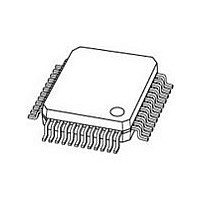
... A2 A3 CDA CDB CS SC68C652B_2 Product data sheet Dual UART with 32-byte FIFOs and IrDA encoder/decoder RXB 4 RXA 5 6 TXRDYB SC68C652BIB48 7 TXA TXB 8 OP2B n.c. 12 Pin configuration for LQFP48 Pin description Pin Type Description 28 I Address 0 select bit. Internal registers address selection. ...
Page 5
... NXP Semiconductors Table 2. Symbol CTSA CTSB DSRA DSRB DTRA DTRB GND IRQ R/W n.c. OP2A OP2B SC68C652B_2 Product data sheet Dual UART with 32-byte FIFOs and IrDA encoder/decoder Pin description …continued Pin Type Description 38 I Clear to Send (active LOW). These inputs are associated with individual UART channels A and B ...
Page 6
... NXP Semiconductors Table 2. Symbol RESET RIA RIB RTSA RTSB RXA RXB RXRDYA RXRDYB TXA TXB TXRDYA TXRDYB SC68C652B_2 Product data sheet Dual UART with 32-byte FIFOs and IrDA encoder/decoder Pin description …continued Pin Type Description 36 I Reset (active LOW). This pin will reset the internal registers and all the outputs ...
Page 7
... NXP Semiconductors Table 2. Symbol V CC XTAL1 XTAL2 SC68C652B_2 Product data sheet Dual UART with 32-byte FIFOs and IrDA encoder/decoder Pin description …continued Pin Type Description 19 Power supply input Crystal or external clock input. Functions as a crystal input external clock input. A crystal can be connected between this pin and XTAL2 to form an internal oscillator circuit (see This confi ...
Page 8
... NXP Semiconductors 6. Functional description The SC68C652B UART is pin-compatible with the SC68C2550B UART. It provides more enhanced features. All additional features are provided through a special enhanced feature register. The UART will perform serial-to-parallel conversion on data characters received from peripheral devices or modems, and parallel-to-parallel conversion on data characters transmitted by the processor ...
Page 9
... NXP Semiconductors 6.2 Internal registers The SC68C652B provides two sets of internal registers (A and B) consisting of 17 registers each for monitoring and controlling the functions of each channel of the UART. These registers are shown in registers (THR/RHR), interrupt status and control registers (IER/ISR), a FIFO control ...
Page 10
... NXP Semiconductors Table 5. Selected trigger level (characters 6.4 Hardware flow control When automatic hardware flow control is enabled, the SC68C652B monitors the CTSn pin for a remote buffer overflow indication and controls the RTSn pin for local buffer overflows. Automatic hardware flow control is selected by setting EFR[6] (RTS) and EFR[7] (CTS logic 1. If CTSn transitions from a logic logic 1 indicating a fl ...
Page 11
... NXP Semiconductors as received data passes the programmed trigger level. To clear this condition, the SC68C652B will transmit the programmed Xon1/Xon2 characters as soon as receive data drops below the programmed trigger level. 6.6 Special feature software flow control A special feature is provided to detect an 8-bit character when EFR[5] is set. When 8-bit character is detected, wit will be placed on the user-accessible data stack along with normal incoming receive data ...
Page 12
... NXP Semiconductors 6.8 Programmable baud rate generator The SC68C652B supports high speed modem technologies that have increased input data rates by employing data compression schemes. For example, a 33.6 kbit/s modem that employs data compression may require a 115.2 kbit/s input data rate. A 128.0 kbit/s ISDN modem that supports data compression may need an input data rate of 460 ...
Page 13
... NXP Semiconductors Table 6. Output baud rate 50 75 110 150 300 600 1200 2400 3600 4800 7200 9600 19.2 k 38.4 k 57.6 k 115.2 k 6.9 DMA operation The SC68C652B FIFO trigger level provides additional flexibility to the user for block mode operation. The user can optionally operate the transmit and receive FIFOs in the DMA mode (FCR[3]) ...
Page 14
... NXP Semiconductors MCR[0] DTR, MCR[3] (OP2) and MCR[2] (OP1). Loopback test data is entered into the transmit holding register via the user data bus interface D7. The transmit UART serializes the data and passes the serial data to the receive UART via the internal loopback connection ...
Page 15
... NXP Semiconductors 7. Register descriptions Table 9 assigned bit functions are more fully defined in Table 9. SC68C652B internal registers [ Register Default [2] General register set RHR THR IER FCR ISR LCR MCR LSR MSR SPR FF [4] Special register set DLL DLM XX [5] Enhanced register set ...
Page 16
... NXP Semiconductors 7.1 Transmit Holding Register (THR) and Receive Holding Register (RHR) The serial transmitter section consists of an 8-bit Transmit Hold Register (THR) and Transmit Shift Register (TSR). The status of the THR is provided in the Line Status Register (LSR). Writing to the THR transfers the contents of the data bus (D[7:0]) to the TSR and UART via the THR, providing that the THR is empty. The THR empty fl ...
Page 17
... NXP Semiconductors Table 10. Bit 7.2.1 IER versus Transmit/Receive FIFO interrupt mode operation When the receive FIFO (FCR[0] = logic 1), and receive interrupts (IER[0] = logic 1) are enabled, the receive interrupts and register status will reflect the following: • The receive RXRDY interrupt (Level 2 ISR interrupt) is issued to the external CPU when the receive FIFO has reached the programmed trigger level ...
Page 18
... NXP Semiconductors 7.2.2 IER versus Receive/Transmit FIFO polled mode operation When FCR[0] = logic 1, resetting IER[0:3] enables the SC68C652B in the FIFO polled mode of operation. In this mode, interrupts are not generated and the user must poll the LSR register for transmit and/or receive data status. Since the receiver and transmitter have separate bits in the LSR either or both can be used in the polled mode by selecting respective transmit or receive control bit(s) ...
Page 19
... NXP Semiconductors 7.3.2 FIFO mode Table 11. Bit 7:6 5 SC68C652B_2 Product data sheet Dual UART with 32-byte FIFOs and IrDA encoder/decoder FIFO Control Register bits description Symbol Description FCR[7:6] RCVR trigger. These bits are used to set the trigger level for the receive FIFO interrupt ...
Page 20
... NXP Semiconductors Table 12. FCR[ Table 13. FCR[ SC68C652B_2 Product data sheet Dual UART with 32-byte FIFOs and IrDA encoder/decoder RCVR trigger levels FCR[6] Receive FIFO trigger level (bytes FIFO trigger levels FCR[4] TX FIFO trigger level (bytes Rev. 02 — 2 November 2009 SC68C652B © NXP B.V. 2009. All rights reserved. ...
Page 21
... NXP Semiconductors 7.4 Interrupt Status Register (ISR) The SC68C652B provides six levels of prioritized interrupts to minimize external software interaction. The Interrupt Status Register (ISR) provides the user with six interrupt status bits. Performing a read cycle on the ISR will provide the user with the highest pending interrupt level to be serviced ...
Page 22
... NXP Semiconductors 7.5 Line Control Register (LCR) The Line Control Register is used to specify the asynchronous data communication format. The word length, the number of stop bits, and the parity are selected by writing the appropriate bits in this register. Table 16. Bit 7 6 5:3 2 1:0 Table 17 ...
Page 23
... NXP Semiconductors 7.6 Modem Control Register (MCR) This register controls the interface with the modem or a peripheral device. Table 20. Bit SC68C652B_2 Product data sheet Dual UART with 32-byte FIFOs and IrDA encoder/decoder Modem Control Register bits description Symbol Description MCR[7] Clock select ...
Page 24
... NXP Semiconductors 7.7 Line Status Register (LSR) This register provides the status of data transfers between the SC68C652B and the CPU. Table 21. Bit SC68C652B_2 Product data sheet Dual UART with 32-byte FIFOs and IrDA encoder/decoder Line Status Register bits description Symbol Description ...
Page 25
... NXP Semiconductors 7.8 Modem Status Register (MSR) This register provides the current state of the control interface signals from the modem, or other peripheral device to which the SC68C652B is connected. Four bits of this register are used to indicate the changed information. These bits are set to a logic 1 whenever a control input from the modem changes state ...
Page 26
... NXP Semiconductors 7.10 Enhanced Feature Register (EFR) Enhanced features are enabled or disabled using this register. Bits 0 through 4 provide single or dual character software flow control selection. When the Xon1 and Xon2 and/or Xoff1 and Xoff2 modes are selected, the double 8-bit words are concatenated into two sequential numbers ...
Page 27
... NXP Semiconductors Table 24. Cont [1] When using a software flow control the Xon/Xoff characters cannot be used for data transfer. 7.11 SC68C652B external reset condition Table 25. Register IER FCR ISR LCR MCR LSR MSR SPR DLL DLM Table 26. Output TXA, TXB OP2A, OP2B RTSA, RTSB ...
Page 28
... NXP Semiconductors 8. Limiting values Table 27. In accordance with the Absolute Maximum Rating System (IEC 60134). Symbol amb T stg P /pack tot SC68C652B_2 Product data sheet Dual UART with 32-byte FIFOs and IrDA encoder/decoder Limiting values Parameter Conditions supply voltage voltage on any other pin ...
Page 29
... NXP Semiconductors 9. Static characteristics Table 28. Static characteristics +85 C; tolerance of V amb Symbol Parameter V clock LOW-level input voltage IL(clk) V clock HIGH-level input voltage IH(clk) V LOW-level input voltage IL V HIGH-level input voltage IH V LOW-level output voltage OL V HIGH-level output voltage OH I LOW-level input leakage ...
Page 30
... NXP Semiconductors 10. Dynamic characteristics Table 29. Dynamic characteristics +85 C; tolerance of V amb Symbol Parameter t R/W to chip select d1 t read cycle delay d2 t delay from CS to data d3 t data disable time d4 t write cycle delay d6 t delay from write to output d7 t delay to set interrupt from modem ...
Page 31
... NXP Semiconductors 10.1 Timing diagrams su1 R Fig 5. General read timing su1 R Fig 6. General write timing SC68C652B_2 Product data sheet Dual UART with 32-byte FIFOs and IrDA encoder/decoder valid address valid data valid address su2 valid data Rev. 02 — 2 November 2009 SC68C652B ...
Page 32
... NXP Semiconductors (1) CS (write) RTSA, RTSB change of state DTRA, DTRB CDA, CDB CTSA, CTSB DSRA, DSRB IRQ (2) CS (read) RIA, RIB (1) CS timing during a write cycle. See (2) CS timing during a read cycle. See Fig 7. Modem input/output timing external clock -------------- - XTAL t w clk Fig 8 ...
Page 33
... NXP Semiconductors RXA, RXB IRQ CS (read) Fig 9. Receive timing RXA, RXB RXRDYA, RXRDYB CS (read) Fig 10. Receive ready timing in non-FIFO mode SC68C652B_2 Product data sheet Dual UART with 32-byte FIFOs and IrDA encoder/decoder Start bit data bits ( data bits 6 data bits 7 data bits ...
Page 34
... NXP Semiconductors RXA, RXB RXRDYA, RXRDYB CS (read) Fig 11. Receive ready timing in FIFO mode TXA, TXB IRQ active CS (write) Fig 12. Transmit timing SC68C652B_2 Product data sheet Dual UART with 32-byte FIFOs and IrDA encoder/decoder Start bit data bits ( Start bit data bits ( ...
Page 35
... NXP Semiconductors TXA, TXB active CS (write byte #1 TXRDYA, TXRDYB Fig 13. Transmit ready timing in non-FIFO mode TXA, TXB CS (write) active byte #32 TXRDYA, TXRDYB Fig 14. Transmit ready timing in FIFO mode SC68C652B_2 Product data sheet Dual UART with 32-byte FIFOs and IrDA encoder/decoder Start ...
Page 36
... NXP Semiconductors start 0 TX data IrDA TX data bit time Fig 15. Infrared transmit timing IrDA RX data bit time RX data Fig 16. Infrared receive timing SC68C652B_2 Product data sheet Dual UART with 32-byte FIFOs and IrDA encoder/decoder UART frame data bits start data bits UART frame Rev. 02 — ...
Page 37
... NXP Semiconductors 11. Package outline LQFP48: plastic low profile quad flat package; 48 leads; body 1 pin 1 index DIMENSIONS (mm are the original dimensions) A UNIT max. 0.20 1.45 1.6 mm 0.25 0.05 1.35 Note 1. Plastic or metal protrusions of 0.25 mm maximum per side are not included. OUTLINE VERSION ...
Page 38
... NXP Semiconductors 12. Soldering of SMD packages This text provides a very brief insight into a complex technology. A more in-depth account of soldering ICs can be found in Application Note AN10365 “Surface mount reflow soldering description” . 12.1 Introduction to soldering Soldering is one of the most common methods through which packages are attached to Printed Circuit Boards (PCBs), to form electrical circuits ...
Page 39
... NXP Semiconductors 12.4 Reflow soldering Key characteristics in reflow soldering are: • Lead-free versus SnPb soldering; note that a lead-free reflow process usually leads to higher minimum peak temperatures (see reducing the process window • Solder paste printing issues including smearing, release, and adjusting the process window for a mix of large and small components on one board • ...
Page 40
... NXP Semiconductors Fig 18. Temperature profiles for large and small components For further information on temperature profiles, refer to Application Note AN10365 “Surface mount reflow soldering description” . 13. Abbreviations Table 32. Acronym CPU DMA FIFO IrDA ISDN LSB MSB UART SC68C652B_2 Product data sheet ...
Page 41
... Modifications: The format of this data sheet has been redesigned to comply with the new identity guidelines of NXP Semiconductors. • Legal texts have been adapted to the new company name where appropriate. • Data sheet title modified from “... and Motorola P interface” to “... and 68 mode P interface” ...
Page 42
... Right to make changes — NXP Semiconductors reserves the right to make changes to information published in this document, including without limitation specifications and product descriptions, at any time and without notice ...
Page 43
... NXP Semiconductors 17. Contents 1 General description . . . . . . . . . . . . . . . . . . . . . . 1 2 Features . . . . . . . . . . . . . . . . . . . . . . . . . . . . . . . 1 3 Ordering information . . . . . . . . . . . . . . . . . . . . . 2 4 Block diagram . . . . . . . . . . . . . . . . . . . . . . . . . . 3 5 Pinning information . . . . . . . . . . . . . . . . . . . . . . 4 5.1 Pinning . . . . . . . . . . . . . . . . . . . . . . . . . . . . . . . 4 5.2 Pin description . . . . . . . . . . . . . . . . . . . . . . . . . 4 6 Functional description . . . . . . . . . . . . . . . . . . . 8 6.1 UART A-B functions . . . . . . . . . . . . . . . . . . . . . 8 6.2 Internal registers 6.3 FIFO operation . . . . . . . . . . . . . . . . . . . . . . . . . 9 6.4 Hardware flow control . . . . . . . . . . . . . . . . . . . 10 6.5 Software flow control . . . . . . . . . . . . . . . . . . . 10 6.6 Special feature software fl ...