PCF8591P NXP Semiconductors, PCF8591P Datasheet - Page 24
PCF8591P
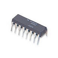
Manufacturer Part Number
PCF8591P
Description
IC, A/D AND D/A CONVERTER, 8BIT, 16-DIP
Manufacturer
NXP Semiconductors
Type
General Purposer
Specifications of PCF8591P
Number Of Channels
1
Number Of Adc's
1
Number Of Dac's
1
Adc/dac Resolution
8b
Interface Type
Serial (I2C)
Operating Supply Voltage (typ)
3.3/5V
Sample Rate
11.1KSPS
Number Of Adc Inputs
4
Number Of Dac Outputs
1
Operating Supply Voltage (max)
6V
Operating Supply Voltage (min)
2.5V
Operating Temperature (max)
85C
Operating Temperature (min)
-40C
Pin Count
16
Mounting
Through Hole
Supply Voltage Range
2.5V To 6V
Operating Temperature Range
-40°C To +85°C
Digital Ic Case Style
DIP
No. Of Pins
16
Linearity Error -
1.5LSB
Termination Type
DIP
Supply Voltage Max
8V
Input Channels Per Adc
1
Rohs Compliant
Yes
Filter Terminals
DIP
Conversion Time
90µs
Data Interface
I2C, Serial
Lead Free Status / RoHS Status
Compliant
Available stocks
Company
Part Number
Manufacturer
Quantity
Price
Company:

Part Number:
PCF8591P
Manufacturer:
SANYO
Quantity:
20 200
Company:
Part Number:
PCF8591P
Manufacturer:
NXP
Quantity:
5 510


Philips Semiconductors
17 SOLDERING
17.1
There is no soldering method that is ideal for all IC
packages. Wave soldering is often preferred when
through-hole and surface mounted components are mixed
on one printed-circuit board. However, wave soldering is
not always suitable for surface mounted ICs, or for
printed-circuits with high population densities. In these
situations reflow soldering is often used.
This text gives a very brief insight to a complex technology.
A more in-depth account of soldering ICs can be found in
our “Data Handbook IC26; Integrated Circuit Packages”
(order code 9398 652 90011).
17.2
17.2.1
The maximum permissible temperature of the solder is
260 C; solder at this temperature must not be in contact
with the joint for more than 5 seconds. The total contact
time of successive solder waves must not exceed
5 seconds.
The device may be mounted up to the seating plane, but
the temperature of the plastic body must not exceed the
specified maximum storage temperature (T
printed-circuit board has been pre-heated, forced cooling
may be necessary immediately after soldering to keep the
temperature within the permissible limit.
17.2.2
Apply a low voltage soldering iron (less than 24 V) to the
lead(s) of the package, below the seating plane or not
more than 2 mm above it. If the temperature of the
soldering iron bit is less than 300 C it may remain in
contact for up to 10 seconds. If the bit temperature is
between 300 and 400 C, contact may be up to 5 seconds.
17.3
17.3.1
Reflow soldering techniques are suitable for all SO
packages.
Reflow soldering requires solder paste (a suspension of
fine solder particles, flux and binding agent) to be applied
to the printed-circuit board by screen printing, stencilling or
pressure-syringe dispensing before package placement.
1998 Jul 02
8-bit A/D and D/A converter
Introduction
DIP
SO
S
R
R
OLDERING BY DIPPING OR BY WAVE
EPAIRING SOLDERED JOINTS
EFLOW SOLDERING
stg max
). If the
24
Several techniques exist for reflowing; for example,
thermal conduction by heated belt. Dwell times vary
between 50 and 300 seconds depending on heating
method. Typical reflow temperatures range from
215 to 250 C.
Preheating is necessary to dry the paste and evaporate
the binding agent. Preheating duration: 45 minutes at
45 C.
17.3.2
Wave soldering techniques can be used for all SO
packages if the following conditions are observed:
During placement and before soldering, the package must
be fixed with a droplet of adhesive. The adhesive can be
applied by screen printing, pin transfer or syringe
dispensing. The package can be soldered after the
adhesive is cured.
Maximum permissible solder temperature is 260 C, and
maximum duration of package immersion in solder is
10 seconds, if cooled to less than 150 C within
6 seconds. Typical dwell time is 4 seconds at 250 C.
A mildly-activated flux will eliminate the need for removal
of corrosive residues in most applications.
17.3.3
Fix the component by first soldering two diagonally-
opposite end leads. Use only a low voltage soldering iron
(less than 24 V) applied to the flat part of the lead. Contact
time must be limited to 10 seconds at up to 300 C. When
using a dedicated tool, all other leads can be soldered in
one operation within 2 to 5 seconds between
270 and 320 C.
A double-wave (a turbulent wave with high upward
pressure followed by a smooth laminar wave) soldering
technique should be used.
The longitudinal axis of the package footprint must be
parallel to the solder flow.
The package footprint must incorporate solder thieves at
the downstream end.
W
R
EPAIRING SOLDERED JOINTS
AVE SOLDERING
Product specification
PCF8591
Related parts for PCF8591P
Image
Part Number
Description
Manufacturer
Datasheet
Request
R

Part Number:
Description:
NXP Semiconductors designed the LPC2420/2460 microcontroller around a 16-bit/32-bitARM7TDMI-S CPU core with real-time debug interfaces that include both JTAG andembedded trace
Manufacturer:
NXP Semiconductors
Datasheet:

Part Number:
Description:
NXP Semiconductors designed the LPC2458 microcontroller around a 16-bit/32-bitARM7TDMI-S CPU core with real-time debug interfaces that include both JTAG andembedded trace
Manufacturer:
NXP Semiconductors
Datasheet:
Part Number:
Description:
NXP Semiconductors designed the LPC2468 microcontroller around a 16-bit/32-bitARM7TDMI-S CPU core with real-time debug interfaces that include both JTAG andembedded trace
Manufacturer:
NXP Semiconductors
Datasheet:
Part Number:
Description:
NXP Semiconductors designed the LPC2470 microcontroller, powered by theARM7TDMI-S core, to be a highly integrated microcontroller for a wide range ofapplications that require advanced communications and high quality graphic displays
Manufacturer:
NXP Semiconductors
Datasheet:
Part Number:
Description:
NXP Semiconductors designed the LPC2478 microcontroller, powered by theARM7TDMI-S core, to be a highly integrated microcontroller for a wide range ofapplications that require advanced communications and high quality graphic displays
Manufacturer:
NXP Semiconductors
Datasheet:
Part Number:
Description:
The Philips Semiconductors XA (eXtended Architecture) family of 16-bit single-chip microcontrollers is powerful enough to easily handle the requirements of high performance embedded applications, yet inexpensive enough to compete in the market for hi
Manufacturer:
NXP Semiconductors
Datasheet:
Part Number:
Description:
The XA-S3 device is a member of Philips Semiconductors? XA(eXtended Architecture) family of high performance 16-bitsingle-chip microcontrollers
Manufacturer:
NXP Semiconductors
Datasheet:

Part Number:
Description:
The NXP BlueStreak LH75401/LH75411 family consists of two low-cost 16/32-bit System-on-Chip (SoC) devices
Manufacturer:
NXP Semiconductors
Datasheet:
Part Number:
Description:
The NXP LPC3130/3131 combine an 180 MHz ARM926EJ-S CPU core, high-speed USB2
Manufacturer:
NXP Semiconductors
Datasheet:
Part Number:
Description:
The NXP LPC3141 combine a 270 MHz ARM926EJ-S CPU core, High-speed USB 2
Manufacturer:
NXP Semiconductors
Part Number:
Description:
The NXP LPC3143 combine a 270 MHz ARM926EJ-S CPU core, High-speed USB 2
Manufacturer:
NXP Semiconductors

Part Number:
Description:
The NXP LPC3152 combines an 180 MHz ARM926EJ-S CPU core, High-speed USB 2
Manufacturer:
NXP Semiconductors
Part Number:
Description:
The NXP LPC3154 combines an 180 MHz ARM926EJ-S CPU core, High-speed USB 2
Manufacturer:
NXP Semiconductors

Part Number:
Description:
Standard level N-channel enhancement mode Field-Effect Transistor (FET) in a plastic package using NXP High-Performance Automotive (HPA) TrenchMOS technology
Manufacturer:
NXP Semiconductors
Datasheet: