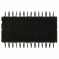
ICS9DB403DGILFT IDT, Integrated Device Technology Inc, ICS9DB403DGILFT Datasheet - Page 7

ICS9DB403DGILFT
Manufacturer Part Number
ICS9DB403DGILFT
Description
IC BUFFER 4OUTPUT DIFF 28-TSSOP
Manufacturer
IDT, Integrated Device Technology Inc
Type
Clock Bufferr
Datasheet
1.ICS9DB403DFLFT.pdf
(19 pages)
Specifications of ICS9DB403DGILFT
Input
HCSL
Output
HCSL, LVDS
Frequency - Max
400MHz
Voltage - Supply
3.135 V ~ 3.465 V
Operating Temperature
-40°C ~ 85°C
Mounting Type
Surface Mount
Package / Case
28-TSSOP
Frequency-max
400MHz
Lead Free Status / RoHS Status
Lead free / RoHS Compliant
Other names
800-1248-2
9DB403DGILFT
9DB403DGILFT
Available stocks
Company
Part Number
Manufacturer
Quantity
Price
Company:
Part Number:
ICS9DB403DGILFT
Manufacturer:
TI
Quantity:
5 325
IDT
T
1
2
3 Measured from differential waveform
4
5
6
Electrical Characteristics - DIF 0.7V Current Mode Differential Pair
Guaranteed by design and characterization, not 100% tested in production.
A
I
See http://www.pcisig.com for complete specs
Device driven by 932S421C or equivalent.
First number is High Bandwidth Mode, second number is Low Bandwidth Mode
Skew, Output to Output
ICS9DB403D
Four Output Differential Buffer for PCIe for Gen 1 and Gen 2
Crossing Voltage (abs)
REF
Current Source Output
Crossing Voltage (var)
TM
Skew, Input to Output
=Tambient; V
Jitter, Cycle to cycle
Rise Time Variation
/ICS
Fall Time Variation
= V
PARAMETER
Voltage High
Jitter, Phase
Max Voltage
Voltage Low
Min Voltage
TM
Impedance
Duty Cycle
Rise Time
Fall Time
DD
Four Output Differential Buffer for PCIe Gen 1 and Gen 2
/(3xR
DD
R
). For R
= 3.3 V +/-5%; C
R
= 475 Ω (1%), I
Vcross(abs)
SYMBOL
d-Vcross
t
t
jphaseBYP
t
jphasePLL
VHigh
VLow
t
jcyc-cyc
Vovs
Vuds
t
pdBYP
pdPLL
Zo
t
d-t
d-t
d
sk3
t
t
t3
r
f
1
r
f
L
=2pF, R
PCIe Gen 2 High Band phase jitter
PCIe Gen 2 High Band phase jitter
Statistical measurement on single
PCIe Gen 2 Low Band phase jitter
PCIe Gen 2 Low Band phase jitter
REF
ended signal using oscilloscope
Additive Jitter in Bypass Mode
Measurement on single ended
Measurement from differential
Variation of crossing over all
V
signal using absolute value.
V
S
(Additive in Bypass Mode)
(Additive in Bypass Mode)
(Additive in Bypass Mode)
= 2.32mA. I
Bypass Mode, V
OL
OH
=33 Ω , R
PCIe Gen 1 phase jitter
PCIe Gen1 phase jitter
PLL Mode V
= 0.175V, V
= 0.525V V
math function.
CONDITIONS
V
PLL mode
wavefrom
P
T
edges
=49.9 Ω , R
= 50%
OH
T
= 6 x I
7
OL
OH
= 50%
T
= 0.175V
= 0.525V
= 50%
REF
REF
=475 Ω
and V
OH
3000
2500
-150
-300
-250
MIN
660
250
175
175
45
= 0.7V @ Z
TYP
2.7/
0.3
1.5
2.2
40
7
0
O
=50 Ω .
ICS9DB403D
MAX
1150
4500
850
150
550
140
700
700
125
125
250
0.1
0.5
3.1
55
50
50
50
10
86
3
(pk2pk)
(pk2pk)
UNITS NOTES
(rms)
(rms)
(rms)
(rms)
mV
mV
mV
mV
ps
ps
ps
ps
ps
ps
ps
ps
ps
ps
ps
ps
ps
%
ps
ps
Ω
REV M 01/27/11
1,4,5,6
1,4,5
1,4,5
1,4,5
1,4,5
1,4,5
1,2
1,2
1,3
1,3
1
1
1
1
1
1
1
1
1
1
1
1
1


