ICS8302AMLF IDT, Integrated Device Technology Inc, ICS8302AMLF Datasheet
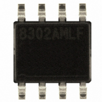
IC CLK FANOUT BUFFER 1:2 8SOIC

ICS8302AMLF

Manufacturer Part Number
ICS8302AMLF
Description
IC CLK FANOUT BUFFER 1:2 8SOIC
Manufacturer
IDT, Integrated Device Technology Inc
Series
HiPerClockS™r
Type
Fanout Buffer (Distribution)r
Datasheets

Specifications of ICS8302AMLF

Number Of Circuits
1
Ratio - Input:output
1:2
Differential - Input:output
No/No
Input
LVCMOS, LVTTL
Output
LVCMOS, LVTTL
Frequency - Max
200MHz
Voltage - Supply
3.135 V ~ 3.465 V
Operating Temperature
0°C ~ 70°C
Mounting Type
Surface Mount
Package / Case
8-SOIC
Frequency-max
200MHz
Number Of Outputs
2
Operating Supply Voltage (max)
3.465V
Operating Temp Range
0C to 70C
Propagation Delay Time
3.3ns
Operating Supply Voltage (min)
3.135V
Mounting
Surface Mount
Pin Count
8
Operating Supply Voltage (typ)
3.3V
Package Type
SOIC N
Duty Cycle
60%
Operating Temperature Classification
Commercial
Lead Free Status / RoHS Status
Lead free / RoHS Compliant
Other names
800-1104
800-1104-5
800-1104
8302AMLF

Available stocks

Company
Part Number
Manufacturer
Quantity
Price
Part Number:
ICS8302AMLF
Manufacturer:
NS/TI
Quantity:
4 500
Part Number:
ICS8302AMLF
Manufacturer:
ICS
Quantity:
20 000
B
8302AM
G
clock input accepts LVCMOS or LVTTL input levels. The
ICS8302 features a pair of LVCMOS/LVTTL outputs. The
I C S 8 3 0 2 i s c h a r a c t e r i ze d a t f u l l 3 . 3 V for input V
and mixed 3.3V and 2.5V for output operating supply
m o d e s (V
skew characteristics make the ICS8302 ideal for clock
distribution applications demanding well defined performance
and repeatibility.
HiPerClockS™
ICS
LOCK
ENERAL
CLK
DDO
D
The ICS8302 is a low skew, 1-to-2 LVCMOS/
LVTTL Fanout Buffer and a member of the
HiPerClock S™ family of High Performance
Clock Solutions from ICS. The ICS8302 has
a single ended clock input. The single ended
). G u a r a n t e e d o u t p u t a n d p a r t - t o - p a r t
IAGRAM
Integrated
Circuit
Systems, Inc.
D
ESCRIPTION
Q0
Q1
www.icst.com/products/hiperclocks.html
DD
,
1
F
• 2 LVCMOS / LVTTL outputs
• LVCMOS / LVTTL clock input accepts LVCMOS
• Maximum output frequency: 200MHz
• Output skew: 25ps (typical)
• Part-to-part skew: 250ps (typical)
• Small 8 lead SOIC package saves board space
• Full 3.3V or 3.3V core, 2.5V supply modes
• 0°C to 70°C ambient operating temperature
• Lead-Free package fully RoHS compliant
P
or LVTTL input levels
EATURES
IN
A
LVCMOS / LVTTL F
SSIGNMENT
3.8mm x 4.8mm, x 1.47mm package body
GND
V
CLK
V
DDO
DD
8-Lead SOIC
ICS8302
M Package
Top View
1
2
3
4
8
7
6
5
L
OW
Q0
GND
V
Q1
DDO
ANOUT
S
ICS8302
KEW
REV. D MAY 17, 2005
, 1-
B
UFFER
TO
-2

Related parts for ICS8302AMLF

ICS8302AMLF Summary of contents

Page 1

Integrated Circuit Systems, Inc ENERAL ESCRIPTION The ICS8302 is a low skew, 1-to-2 LVCMOS/ ICS LVTTL Fanout Buffer and a member of the HiPerClockS™ HiPerClock S™ family of High Performance Clock Solutions from ICS. The ICS8302 has a ...

Page 2

Integrated Circuit Systems, Inc ABLE IN ESCRIPTIONS ...

Page 3

Integrated Circuit Systems, Inc BSOLUTE AXIMUM ATINGS Supply Voltage Inputs, V -0. Outputs, V -0. Package Thermal Impedance, JA Storage Temperature, T -65°C to 150°C STG T 3A. P ...

Page 4

Integrated Circuit Systems, Inc ABLE OWER UPPLY HARACTERISTICS ...

Page 5

Integrated Circuit Systems, Inc. P ARAMETER 1.65V± DDO LVCMOS GND -1.65V±5% 3. UTPUT OAD EST IRCUIT PART PART tsk(pp ...

Page 6

Integrated Circuit Systems, Inc ABLE VS IR LOW ABLE FOR JA Single-Layer PCB, JEDEC Standard Test Boards Multi-Layer PCB, JEDEC Standard Test Boards NOTE: Most modern PCB designs use multi-layered boards. The ...

Page 7

Integrated Circuit Systems, Inc ACKAGE UTLINE UFFIX FOR EAD T Reference Document: JEDEC Publication 95, MS-012 8302AM LVCMOS / LVTTL F SOIC ABLE ACKAGE IMENSIONS ...

Page 8

Integrated Circuit Systems, Inc ABLE RDERING NFORMATION ...

Page 9

Integrated Circuit Systems, Inc & T ...

Related keywords