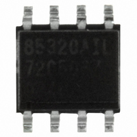
ICS85320AMILF IDT, Integrated Device Technology Inc, ICS85320AMILF Datasheet - Page 7

ICS85320AMILF
Manufacturer Part Number
ICS85320AMILF
Description
IC TRANSLATOR LVPECL 8-SOIC
Manufacturer
IDT, Integrated Device Technology Inc
Type
Translatorr
Datasheet
1.ICS85320AMILF.pdf
(16 pages)
Specifications of ICS85320AMILF
Number Of Circuits
1
Ratio - Input:output
1:1
Differential - Input:output
No/Yes
Input
LVCMOS, LVTTL
Output
LVPECL
Frequency - Max
267MHz
Voltage - Supply
2.375 V ~ 3.465 V
Operating Temperature
-40°C ~ 85°C
Mounting Type
Surface Mount
Package / Case
8-SOIC
Frequency-max
267MHz
Number Of Outputs
2
Operating Supply Voltage (max)
3.465V
Operating Temp Range
-40C to 85C
Propagation Delay Time
1.7ns
Operating Supply Voltage (min)
2.375V
Mounting
Surface Mount
Pin Count
8
Operating Supply Voltage (typ)
2.5/3.3V
Package Type
SOIC N
Duty Cycle
55%
Operating Temperature Classification
Industrial
Lead Free Status / RoHS Status
Lead free / RoHS Compliant
Other names
800-1168
800-1168-5
800-1168
85320AMILF
800-1168-5
800-1168
85320AMILF
Available stocks
Company
Part Number
Manufacturer
Quantity
Price
Company:
Part Number:
ICS85320AMILF
Manufacturer:
IDT Integrated Device Technolo
Quantity:
135
Part Number:
ICS85320AMILF
Manufacturer:
IDT
Quantity:
20 000
T
The clock layout topology shown below is a typical termination
for LVPECL outputs. The two different layouts mentioned are
recommended only as guidelines.
FOUT and nFOUT are low impedance follower outputs that gen-
erate ECL/LVPECL compatible outputs. Therefore, terminating
resistors (DC current path to ground) or current sources must be
used for functionality. These outputs are designed to drive 50
IDT
RTT =
ERMINATION FOR
ICS85320I
LVCMOS/LVTTL-TO-DIFFERENTIAL 3.3V, 2.5V LVPECL TRANSLATOR
™
/ ICS
((V
F
™
FOUT
OH
IGURE
3.3V, 2.5V LVPECL TRANSLATOR
+ V
OL
1A. LVPECL O
) / (V
1
LVPECL O
CC
Z
Z
– 2)) – 2
o
o
= 50
= 50
Z
o
50
UTPUT
UTPUTS
T
RTT
ERMINATION
50
A
V
PPLICATION
CC
FIN
- 2V
7
I
NFORMATION
transmission lines. Matched impedance techniques should be
used to maximize operating frequency and minimize signal dis-
tortion. Figures 1A and 1B show two different layouts which are
recommended only as guidelines. Other suitable clock layouts
may exist and it would be recommended that the board design-
ers simulate to guarantee compatibility across all printed circuit
and clock component process variations.
FOUT
F
IGURE
1B. LVPECL O
Z
Z
o
o
= 50
= 50
ICS8532AMI REV A NOVEMBER 13, 2006
125
84
UTPUT
3.3V
125
84
T
ERMINATION
FIN


