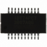
IDT74FCT3807AQG IDT, Integrated Device Technology Inc, IDT74FCT3807AQG Datasheet - Page 2

IDT74FCT3807AQG
Manufacturer Part Number
IDT74FCT3807AQG
Description
IC CLK FAN BUFF 1:10 20QSOP
Manufacturer
IDT, Integrated Device Technology Inc
Series
74FCTr
Type
Fanout Buffer (Distribution)r
Datasheet
1.IDT74FCT3807AQG8.pdf
(8 pages)
Specifications of IDT74FCT3807AQG
Number Of Circuits
1
Ratio - Input:output
1:10
Differential - Input:output
No/No
Input
LVTTL
Output
CMOS, TTL
Frequency - Max
100MHz
Voltage - Supply
3 V ~ 3.6 V
Operating Temperature
0°C ~ 70°C
Mounting Type
Surface Mount
Package / Case
20-QSOP
Frequency-max
100MHz
Number Of Outputs
10
Operating Supply Voltage (max)
3.6V
Operating Temp Range
0C to 70C
Propagation Delay Time
4.3ns
Operating Supply Voltage (min)
3V
Mounting
Surface Mount
Pin Count
20
Operating Supply Voltage (typ)
3.3V
Package Type
QSOP
Quiescent Current
10uA
Input Frequency
133MHz
Operating Temperature Classification
Commercial
Lead Free Status / RoHS Status
Lead free / RoHS Compliant
Other names
74FCT3807AQG
800-1631
800-1631-5
800-1631
800-1631
800-1631-5
800-1631
Available stocks
Company
Part Number
Manufacturer
Quantity
Price
Part Number:
IDT74FCT3807AQG
Manufacturer:
IDT
Quantity:
20 000
Company:
Part Number:
IDT74FCT3807AQG8
Manufacturer:
IDT10
Quantity:
1 938
Part Number:
IDT74FCT3807AQGI
Manufacturer:
IDT
Quantity:
20 000
ABSOLUTE MAXIMUM RATINGS
NOTES:
1. Stresses greater than those listed under ABSOLUTE MAXIMUM RATINGS may cause
2. V
3. Input terminals.
4. Outputs and I/O terminals.
POWER SUPPLY CHARACTERISTICS
NOTES:
1. For conditions shown as Max. or Min., use appropriate value specified under Electrical Characteristics for the applicable device type.
2. Typical values are at V
3. Per TTL driven input (V
4. This parameter is not directly testable, but is derived for use in Total Power Supply calculations.
5. Values for these conditions are examples of the I
6.
IDT74FCT3807/A
3.3V CMOS 1-TO-10 CLOCK DRIVER
Symbol
V
V
V
Symbol
I
I
I
∆I
D
N
I
f
All currents are in milliamps and all frequencies are in megahertz.
C
C
CC
CCD
i
TERM (2)
TERM (3)
TERM (4)
permanent damage to the device. This is a stress rating only and functional operation
of the device at these or any other conditions above those indicated in the operational
sections of this specification is not implied. Exposure to absolute maximum rating
conditions for extended periods may affect reliability.
T
∆I
I
I
H
T
OUT
CCD
= Input Frequency
CC
CC
= I
= I
STG
I
C
CC
= Number of TTL Inputs at D
= Quiescent Current (I
= Duty Cycle for TTL Inputs High
QUIESCENT
CC
= Dynamic Current Caused by an Input Transition Pair (HLH or LHL)
= Power Supply Current for a TTL High Input (V
terminals.
+ ∆I
CC
Description
Terminal Voltage with Respect to GND
Terminal Voltage with Respect to GND
Terminal Voltage with Respect to GND
Storage Temperature
DC Output Current
+ I
D
Parameter
Quiescent Power Supply Current
TTL Inputs HIGH
Dynamic Power Supply Current
Total Power Supply Current
H
INPUTS
N
T
+ I
CC
+ I
CCD
IN
CCL
DYNAMIC
= V
= 3.3V, +25°C ambient.
(f
, I
CC
i
)
CCH
H
-0.6V); all other inputs at V
and I
CCZ
)
(6)
C
(4)
formula. These limits are guaranteed but not tested.
I
N
= V
–0.5 to V
–0.5 to +4.6
–65 to +150
CC
–60 to +60
–0.5 to +7
CC
-0.6V)
Max
or GND.
Test Conditions
V
V
V
Input toggling
50% Duty Cycle
Outputs Open
V
Input toggling
50% Duty Cycle
Outputs Open
fi = 50MHz
CC
IN
CC
CC
CC
= V
(1)
+0.5
= Max.
= Max.
= Max.
CC –
0.6V
Unit
mA
°C
V
V
V
(3)
(1)
2
CAPACITANCE (T
NOTE:
1. This parameter is measured at characterization but not tested.
PIN DESCRIPTION
Symbol
C
C
OUT
IN
Pin Names
O x
I N
COMMERCIAL/INDUSTRIAL TEMPERATURE RANGES
V
V
V
V
V
V
Parameter
Input Capacitance
Output Capacitance
IN
IN
IN
IN
IN
IN
= V
= V
= V
= GND
= GND
= GND
CC –
CC
CC
(1)
0.6V
Clock Inputs
Clock Outputs
A
= +25
Min.
Conditions
—
—
—
—
V
V
OUT
IN
Description
= 0V
= 0V
O
C, f = 1.0MHz)
Typ.
0.31
15.5
15.5
10
(2)
Typ.
4.5
5.5
Max.
0.45
22.8
22.8
30
Max.
6
8
MHz
Unit
mA/
Unit
µA
mA
pF
pF


