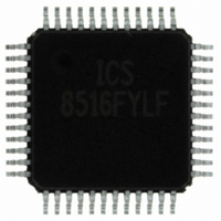
ICS8516FYLF IDT, Integrated Device Technology Inc, ICS8516FYLF Datasheet - Page 9

ICS8516FYLF
Manufacturer Part Number
ICS8516FYLF
Description
IC CLK DISTR 1:16 LVDS 48-LQFP
Manufacturer
IDT, Integrated Device Technology Inc
Series
HiPerClockS™r
Type
Fanout Buffer (Distribution)r
Datasheet
1.ICS8516FYLF.pdf
(16 pages)
Specifications of ICS8516FYLF
Number Of Circuits
1
Ratio - Input:output
1:16
Differential - Input:output
Yes/Yes
Input
HCSL, LVDS, LVHSTL, LVPECL, SSTL
Output
LVDS
Frequency - Max
700MHz
Voltage - Supply
3.135 V ~ 3.465 V
Operating Temperature
0°C ~ 70°C
Mounting Type
Surface Mount
Package / Case
48-LQFP
Frequency-max
700MHz
Number Of Outputs
32
Operating Supply Voltage (max)
3.465V
Operating Temp Range
0C to 70C
Propagation Delay Time
5ns
Operating Supply Voltage (min)
3.135V
Mounting
Surface Mount
Pin Count
48
Operating Supply Voltage (typ)
3.3V
Package Type
TQFP
Duty Cycle
55%
Operating Temperature Classification
Commercial
Lead Free Status / RoHS Status
Lead free / RoHS Compliant
Other names
800-1154
8516FYLF
8516FYLF
Available stocks
Company
Part Number
Manufacturer
Quantity
Price
Company:
Part Number:
ICS8516FYLF
Manufacturer:
AD
Quantity:
1 722
Company:
Part Number:
ICS8516FYLF
Manufacturer:
IDT, Integrated Device Technology Inc
Quantity:
10 000
Company:
Part Number:
ICS8516FYLFT
Manufacturer:
IDT, Integrated Device Technology Inc
Quantity:
10 000
IDT™ / ICS™ LOW SKEW, 1-TO-16 DIFFERENTIAL-TO-LVDS CLOCK DISTRIBUTION CHIP
ICS8516
LOW SKEW, 1-TO-16 DIFFERENTIAL-TO-LVDS CLOCK DISTRIBUTION CHIP
W
Figure 1 shows how the differential input can be wired to accept
single ended levels. The reference voltage V_REF = V
generated by the bias resistors R1, R2 and C1. This bias circuit
should be located as close as possible to the input pin. The ratio
R
I
LVCMOS C
All control pins have internal pull-ups or pull-downs; additional
resistance is not required but can be added for additional
protection. A 1kΩ resistor can be used.
8516FY
NPUTS
ECOMMENDATIONS FOR
IRING THE
:
ONTROL
D
Integrated
Circuit
Systems, Inc.
IFFERENTIAL
P
INS
:
U
NUSED
I
F
NPUT TO
IGURE
I
NPUT AND
1. S
Single Ended Clock Input
A
A
www.icst.com/products/hiperclocks.html
PPLICATION
CCEPT
INGLE
O
E
S
NDED
UTPUT
C1
0.1u
INGLE
D
V_REF
DD
/2 is
IFFERENTIAL
S
IGNAL
P
E
INS
9
9
I
NDED
of R1 and R2 might need to be adjusted to position the V_REF in
the center of the input voltage swing. For example, if the input
clock swing is only 2.5V and V
and R2/R1 = 0.609.
NFORMATION
O
LVDS – Like O
All unused LVDS output pairs can be either left floating or
terminated with 100Ω across. If they are left floating, we
recommend that there is no trace attached.
1K
D
R1
1K
R2
UTPUTS
RIVING
VDD
L
EVELS
nCLKx
CLKx
-
TO
D
:
IFFERENTIAL
-LVDS C
UTPUT
I
NPUT
LOCK
DD
= 3.3V, V_REF should be 1.25V
L
OW
D
ISTRIBUTION
S
KEW
REV. B FEBRUARY 21, 2006
, 1-
TO
C
-16
HIP
ICS8516
TSD


