LV810RIT IDT, Integrated Device Technology Inc, LV810RIT Datasheet
LV810RIT
Specifications of LV810RIT


Related parts for LV810RIT


LV810RIT Summary of contents
Page 1
BUFFER/CLOCK DRIVER Description The ICSLV810 is a low skew 1 2.5 V, 1:10 fanout buffer. This device is specifically designed for data communications clock management. The large fanout from a single input line reduces loading on the input ...
Page 2
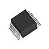
ICSLV810 BUFFER/CLOCK DRIVER Pin Assignment 1 CLKIN 2 GND 3 CLK 1 4 VDDA CLK 2 5 GND 6 7 CLK 3 8 VDDA CLK GND 20 pin (150mil) SSOP Pin Descriptions Pin Pin Number Name 1 ...
Page 3
ICSLV810 BUFFER/CLOCK DRIVER External Components The ICSLV810 requires a minimum number of external components for proper operation. Decoupling Capacitors Decoupling capacitors of 0.01µF must be connected between VDD and GND, as close to these pins as possible. For optimum device ...
Page 4
ICSLV810 BUFFER/CLOCK DRIVER DC Electrical Characteristics—CLKIN and Bank A VDDA = 2.5 V, Ambient Temperature - +85 C Parameter Operating Voltage Quiescent Power Supply Current Short Circuit Current Input High Voltage, CLKIN Input Low Voltage, CLKIN Output High ...
Page 5
ICSLV810 BUFFER/CLOCK DRIVER Parameter Symbol Output High Voltage Output Low Voltage Input High Current Input Low Current Input High Current Input Capacitance Output Capacitance C Note1: This parameter is not tested, guaranteed by design. DC Electrical Characteristics—Bank C VDDC = ...
Page 6
ICSLV810 BUFFER/CLOCK DRIVER Parameter Symbol Input High Current Input Capacitance Output Capacitance C Note1: This parameter is not tested, guaranteed by design. AC Electrical Characteristics—Bank A VDDA = 2.5 V, Ambient Temperature - +85 C Parameter Output Skew: ...
Page 7
ICSLV810 BUFFER/CLOCK DRIVER AC Electrical Characteristics—Bank B VDDB = 2.5 V, Ambient Temperature - +85 C, unless otherwise noted Parameter Output Skew: skew between outputs of same package Pulse Skew: skew between opposite transitions of same output (t ...
Page 8
ICSLV810 BUFFER/CLOCK DRIVER AC Electrical Characteristics—Bank C VDDC = 2.5 V, Ambient Temperature - +85 C, unless otherwise noted Parameter Output Skew: skew between outputs of same package Pulse Skew: skew between opposite transitions of same output (t ...
Page 9
ICSLV810 BUFFER/CLOCK DRIVER Thermal Characteristics for 20QSOP Parameter Thermal Resistance Junction to Ambient Thermal Resistance Junction to Case Thermal Characteristics for 20SOIC Parameter Thermal Resistance Junction to Ambient Thermal Resistance Junction to Case IDT™ / ICS™ BUFFER/CLOCK DRIVER Symbol Conditions ...
Page 10
ICSLV810 BUFFER/CLOCK DRIVER From O utput Under Test CL=3pF Figure 1. Load Circuit Input t PLH Output Figure 2. Propagation Delay Input t PLH1 Output Output 2 t PLH2 ( t =| SK(O) ...
Page 11
ICSLV810 BUFFER/CLOCK DRIVER Package Outline and Package Dimensions Package dimensions are kept current with JEDEC Publication No INDEX AREA IDT™ / ICS™ BUFFER/CLOCK DRIVER (20-pin QSOP, 150 Mil. Body) Symbol E1 E ...
Page 12
ICSLV810 BUFFER/CLOCK DRIVER Package Outline and Package Dimensions Package dimensions are kept current with JEDEC Publication No INDEX AREA Ordering Information Part / Order Number Marking LV810RILF LV810RILF LV810RILFT LV810RILF LV810FILF LV810FILF ...
Page 13
ICSLV810 BUFFER/CLOCK DRIVER Revision History Rev. Originator Date Description of Change A P.Griffith 03/25/05 New device/datasheet. B P.Griffith 05/02/05 Released from Preliminary to final; changed Short Circuit Current parameter in 2 Char table to ±80 mA; changed Short ...
Page 14
ICSLV810 BUFFER/CLOCK DRIVER Innovate with IDT and accelerate your future networks. Contact: www.IDT.com For Sales 800-345-7015 408-284-8200 Fax: 408-284-2775 Corporate Headquarters Integrated Device Technology, Inc. www.idt.com © 2006 Integrated Device Technology, Inc. All rights reserved. Product specifications subject to change ...