MPC9447AC IDT, Integrated Device Technology Inc, MPC9447AC Datasheet

IC CLK FANOUT BUFFER 1:9 32-LQFP

MPC9447AC

Manufacturer Part Number
MPC9447AC
Description
IC CLK FANOUT BUFFER 1:9 32-LQFP
Manufacturer
IDT, Integrated Device Technology Inc
Type
Fanout Buffer (Distribution), Multiplexerr
Datasheet

Specifications of MPC9447AC

Number Of Circuits
1
Ratio - Input:output
2:9
Differential - Input:output
No/No
Input
LVCMOS
Output
LVCMOS
Frequency - Max
350MHz
Voltage - Supply
2.375 V ~ 3.465 V
Operating Temperature
-40°C ~ 85°C
Mounting Type
Surface Mount
Package / Case
32-LQFP
Frequency-max
350MHz
Number Of Clock Inputs
2
Mode Of Operation
Single-Ended
Output Frequency
350MHz
Output Logic Level
LVCMOS
Operating Supply Voltage (min)
2.375V
Operating Supply Voltage (typ)
2.5/3.3V
Operating Supply Voltage (max)
3.465V
Package Type
TQFP
Operating Temp Range
-40C to 85C
Operating Temperature Classification
Industrial
Signal Type
LVCMOS
Mounting
Surface Mount
Pin Count
32
Quiescent Current
2mA
Lead Free Status / RoHS Status
Lead free / RoHS Compliant

Available stocks

Company
Part Number
Manufacturer
Quantity
Price
Part Number:
MPC9447AC
Manufacturer:
IDT, Integrated Device Technology Inc
Quantity:
10 000
Part Number:
MPC9447ACR2
Manufacturer:
IDT, Integrated Device Technology Inc
Quantity:
10 000
fanout buffer targeted for high performance clock tree applications. With output frequencies up
to 350 MHz and output skews less than 150 ps, the device meets the needs of most demanding
clock applications.
Features
Functional Description
precise copy of the input signal with a near zero skew. The outputs buffers support driving of 50 Ω terminated transmission lines on the incident
edge. Each is capable of driving either one parallel terminated or two series terminated transmission lines.
MPC9447 CLK_STOP control is synchronous to the falling edge of the input clock. It allows the start and stop of the output clock signal only
in a logic low state, and thus, eliminates potential output runt pulses. Applying the OE control will force the outputs into high-impedance mode.
V power supply and an ambient temperature range of -40°C to +85°C. The MPC9447 is pin and function compatible but performance-enhanced
to the MPC947.
MPC9447 REVISION 6 APRIL 13, 2010
The Freescale Semiconductor, Inc. MPC9447 is a 3.3 V or 2.5 V compatible, 1:9 clock
MPC9447 is specifically designed to distribute LVCMOS compatible clock signals up to a frequency of 350 MHz. Each output provides a
Two selectable independent LVCMOS compatible clock inputs are available, providing support of redundant clock source systems. The
All inputs have an internal pull-up or pull-down resistor preventing unused and open inputs from floating. The device supports a 2.5 V or 3.3
9 LVCMOS Compatible Clock Outputs
2 Selectable, LVCMOS Compatible Inputs
Maximum Clock Frequency of 350 MHz
Maximum Clock Skew of 150 ps
Synchronous Output Stop in Logic Low State Eliminates Output Runt Pulses
High-Impedance Output Control
3.3 V or 2.5 V Power Supply
Drives up to 18 Series Terminated Clock Lines
Ambient Temperature Range -40°C to +85°C
32-Lead LQFP Packaging
32-lead Pb-free Package Available
Supports Clock Distribution in Networking, Telecommunications, and Computer
Applications
Pin and Function Compatible to MPC947
3.3V, 2.5V, 1:9 LVCMOS Clock Fanout Buffer
1
CLOCK FANOUT BUFFER
©2010 Integrated Device Technology, Inc.
3.3 V/2.5 V LVCMOS 1:9
32-LEAD LQFP PACKAGE
Pb-FREE PACKAGE
LOW VOLTAGE
CASE 873A-03
CASE 873A-03
FA SUFFIX
AC SUFFIX
DATA SHEET
MPC9447

Related parts for MPC9447AC

MPC9447AC Summary of contents

Page 1

LVCMOS Clock Fanout Buffer The Freescale Semiconductor, Inc. MPC9447 2.5 V compatible, 1:9 clock fanout buffer targeted for high performance clock tree applications. With output frequencies up to 350 MHz and output ...

Page 2

MPC9447 Data Sheet V CC CCLK0 0 CLK Stop CCLK1 25k CLK_SE 25k SYNC CLK_STO (All input resistors have a value of 25 kΩ) OE Figure 1. Logic Diagram Table 1. ...

Page 3

MPC9447 Data Sheet Table 3. General Specifications Symbol Characteristics V Output Termination Voltage TT MM ESD Protection (Machine model) HBM ESD Protection (Human body model) LU Latch-up Immunity C Power Dissipation Capacitance PD C Input Capacitance IN Table 4. Absolute ...

Page 4

MPC9447 Data Sheet Table 6. AC Characteristics (V = 3.3 V ± 5 Symbol Characteristics f Input Frequency ref f Output Frequency max f Reference Input Pulse Width P,REF CCLK0, CCLK1 Input Rise/Fall Time r ...

Page 5

MPC9447 Data Sheet Table 8. AC Characteristics (V = 2.5 V ± 5 Symbol Characteristics f Input Frequency ref f Output Frequency max f Reference Input Pulse Width P,REF CCLK0, CCLK1 Input Rise/Fall Time r ...

Page 6

MPC9447 Data Sheet CCLK0 or CCLK1 CLK_STOP Figure 3. Output Clock Stop (CLK_STOP) Timing Diagram Driving Transmission Lines The MPC9447 clock driver was designed to drive high-speed signals in a terminated transmission line environment. To provide the ...

Page 7

MPC9447 Data Sheet Since this step is well above the threshold region, it will not cause any false clock triggering; however, designers may be uncomfortable with unwanted reflections on the line. To better match the impedances when driving multiple lines, ...

Page 8

MPC9447 Data Sheet t SK(LH) The pin-to-pin skew is defined as the worst case difference in propagation delay between any similar delay path within a single device. Figure 9. Output-to-Output Skew ...

Page 9

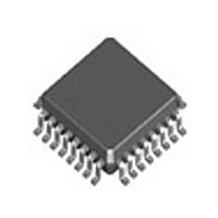
MPC9447 Data Sheet PIN 1 INDEX E1 D/2 4X 0. 28X SEATING PLANE (S) A1 DETAIL AD MPC9447 REVISION 6 APRIL 13, 2010 PACKAGE ...

Page 10

MPC9447 Data Sheet 6024 Silver Creek Valley Road Sales 800-345-7015 (inside USA) San Jose, California 95138 +408-284-8200 (outside USA) Fax: 408-284-2775 www.IDT.com/go/contactIDT DISCLAIMER Integrated Device Technology, Inc. (IDT) and its subsidiaries reserve the right to modify the products and/or specifications ...

Related keywords