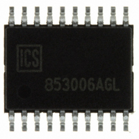
ICS853006AGLF IDT, Integrated Device Technology Inc, ICS853006AGLF Datasheet - Page 8

ICS853006AGLF
Manufacturer Part Number
ICS853006AGLF
Description
IC FANOUT BUFFER LVPECL 20-TSSOP
Manufacturer
IDT, Integrated Device Technology Inc
Series
HiPerClockS™r
Type
Fanout Buffer (Distribution)r
Specifications of ICS853006AGLF
Number Of Circuits
1
Ratio - Input:output
1:6
Differential - Input:output
Yes/Yes
Input
CML, LVDS, LVPECL, SSTL
Output
ECL, LVPECL
Frequency - Max
2GHz
Voltage - Supply
2.375 V ~ 3.465 V
Operating Temperature
-40°C ~ 85°C
Mounting Type
Surface Mount
Package / Case
20-TSSOP
Frequency-max
2GHz
Number Of Outputs
12
Operating Supply Voltage (max)
-3.465/3.465V
Operating Temp Range
-40C to 85C
Propagation Delay Time
0.51ns
Operating Supply Voltage (min)
-2.375/2.375V
Mounting
Surface Mount
Pin Count
20
Operating Supply Voltage (typ)
-2.5/-3.3/3.3V
Package Type
TSSOP
Operating Temperature Classification
Industrial
Lead Free Status / RoHS Status
Lead free / RoHS Compliant
Other names
800-1157
800-1157-5
800-1157
853006AGLF
800-1157-5
800-1157
853006AGLF
IDT™ / ICS™ LOW SKEW, 1-TO-6 DIFFERENTIAL-TO-2.5V/3.3V LVPECL/ECL FANOUT BUFFER
ICS853006
LOW SKEW, 1-TO-6 DIFFERENTIAL-TO-2.5V/3.3V LVPECL/ECL FANOUT BUFFER
T
W
Figure 1 shows an example of the differential input that can be
wired to accept single ended levels. The reference voltage level
V
The clock layout topology shown below is a typical termina-
tion for LVPECL outputs. The two different layouts mentioned
are recommended only as guidelines.
FOUT and nFOUT are low impedance follower outputs that gen-
erate ECL/LVPECL compatible outputs. Therefore, terminating
resistors (DC current path to ground) or current sources must
be used for functionality. These outputs are designed to drive
853006AG
RTT =
BB
ERMINATION FOR
IRING THE
generated from the device is connected to the negative input.
((V
F
FOUT
IGURE
OH
+ V
D
OL
Integrated
Circuit
Systems, Inc.
2A. LVPECL O
IFFERENTIAL
) / (V
1
3.3V LVPECL O
CC
Z
Z
– 2)) – 2
o
o
= 50
= 50
I
F
Z
NPUT TO
IGURE
o
50
UTPUT
1. S
D
A
T
RTT
ERMINATION
IFFERENTIAL
A
UTPUTS
50
PPLICATION
www.icst.com/products/hiperclocks.html
CCEPT
INGLE
CLK_IN
V
CC
FIN
- 2V
E
C1
0.1u
S
NDED
INGLE
-
S
TO
IGNAL
E
8
-2.5V/3.3V LVPECL/ECL F
8
I
NDED
PCLK
VBB
nPCLK
50 transmission lines. Matched impedance techniques should
be used to maximize operating frequency and minimize signal
distortion. Figures 2A and 2B show two different layouts which
are recommended only as guidelines. Other suitable clock lay-
outs may exist and it would be recommended that the board
designers simulate to guarantee compatibility across all printed
circuit and clock component process variations.
NFORMATION
The C1 capacitor should be located as close as possible to the
input pin.
VCC
D
RIVING
L
FOUT
EVELS
F
IGURE
D
IFFERENTIAL
2B. LVPECL O
Z
Z
o
o
= 50
= 50
I
NPUT
125
84
UTPUT
L
OW
3.3V
125
84
T
ANOUT
REV. A NOVEMBER 9, 2004
S
ERMINATION
KEW
FIN
, 1-
B
UFFER
TO
ICS853006
-6
TSD


