ICS525-01RLF IDT, Integrated Device Technology Inc, ICS525-01RLF Datasheet
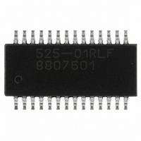
IC CLK USER CONFIGURABLE 28-SSOP

ICS525-01RLF

Manufacturer Part Number
ICS525-01RLF
Description
IC CLK USER CONFIGURABLE 28-SSOP
Manufacturer
IDT, Integrated Device Technology Inc
Series
OSCaR™r
Type
Clock Generator, Fanout Distributionr
Datasheet

Specifications of ICS525-01RLF

Pll
Yes with Bypass
Input
Clock, Crystal
Output
CMOS
Number Of Circuits
1
Ratio - Input:output
1:2
Differential - Input:output
No/No
Frequency - Max
160MHz
Divider/multiplier
Yes/No
Voltage - Supply
3 V ~ 5.5 V
Operating Temperature
0°C ~ 70°C
Mounting Type
Surface Mount
Package / Case
28-SSOP
Frequency-max
160MHz
Number Of Elements
1
Supply Current
8mA
Pll Input Freq (min)
2MHz
Pll Input Freq (max)
50MHz
Operating Supply Voltage (typ)
3.3/5V
Operating Temp Range
0C to 70C
Package Type
QSOP
Output Frequency Range
3 to 160MHz
Operating Supply Voltage (min)
3V
Operating Supply Voltage (max)
5.5V
Operating Temperature Classification
Commercial
Pin Count
28
Lead Free Status / RoHS Status
Lead free / RoHS Compliant
Other names
525-01RLF
800-1047
800-1047-5
800-1047

Available stocks

Company
Part Number
Manufacturer
Quantity
Price
Part Number:
ICS525-01RLF
Manufacturer:
LTC
Quantity:
221
Part Number:
ICS525-01RLF
Manufacturer:
ICS
Quantity:
18
Part Number:
ICS525-01RLF
Manufacturer:
IDT
Quantity:
20 000
Part Number:
ICS525-01RLFT
Manufacturer:
TNTEGRATED
Quantity:
20 000
MDS 525-01/02 T
Description
The ICS525-01/02 are the most flexible way to
generate a high-quality, high-accuracy, high-frequency
clock output from an inexpensive crystal or clock input.
The name OSCaR stands for OSCillator Replacement,
as they are designed to replace crystal oscillators in
almost any electronic system. The user can configure
the device to produce nearly any output frequency from
any input frequency by grounding or floating the select
pins. Neither microcontroller, software, nor device
programmer are needed to set the frequency. Using
Phase-Locked Loop (PLL) techniques, the device
accepts a standard fundamental mode, inexpensive
crystal to produce output clocks up to 250 MHz. It can
also produce a highly accurate output clock from a
given input clock, keeping them frequency locked
together.
For similar capability with a serial interface, use the
ICS307. For simple multipliers to produce common
frequencies, refer to the LOCO
are smaller and more cost effective.
This product is intended for clock generation. It has low
output jitter (variation in the output period), but input to
output skew and jitter are not defined nor guaranteed.
For applications which require defined input to output
timing, use the ICS527-01.
Block Diagram
Crystal or clock
input
Optional crystal capacitors
X1/ICLK
X2
PD
Oscillator
Crystal
TM
Integrated Device Technology, Inc.
family of parts, which
Reference
R6:R0
Divider
7
1
Phase Comparator,
Charge Pump, and
Loop Filter
OSCaR
Divider
V8:V0
9
VCO
Features
Packaged as 28-pin SSOP (150 mil body)
Pb (lead) free package
ICS525-01 with output frequencies up to 160 MHz
ICS525-02 with output frequencies up to 250 MHz
User determines the output frequency by setting all
internal dividers
Eliminates need for custom oscillators
No software needed
Online ICS525 calculator at:
www.idt.com/?app=calculators&source=support_menu
Pull-ups on all select inputs
Input crystal frequency of 5 - 27 MHz
Input clock frequency of 2 - 50 MHz
Very low jitter
Duty cycle of 45/55 up to 200 MHz
Operating voltage of 3.0 V or 5.5 V
Ideal for oscillator replacement
Industrial temperature version available
For Zero Delay, refer to the ICS527
2
2
VDD
GND
www.idt.com
TM
VCO
User Configurable Clock
ICS525-01/02
Divider
S2:S0
Output
3
Revision 081810
CLK
REF

Related parts for ICS525-01RLF

ICS525-01RLF Summary of contents

Page 1

... Description The ICS525-01/02 are the most flexible way to generate a high-quality, high-accuracy, high-frequency clock output from an inexpensive crystal or clock input. The name OSCaR stands for OSCillator Replacement, as they are designed to replace crystal oscillators in almost any electronic system. The user can configure the device to produce nearly any output frequency from any input frequency by grounding or floating the select pins ...

Page 2

... Pin Assignment VDD 6 23 X1/ICLK GND ICS525-01 ICS525-01 Pin Descriptions Pin Pin Pin Number Name Type 1, 2, R5, R6, I(PU) 24-28 R0- S0, S1, S2 I(PU VDD Power 7 X1/ICLK GND Power I(PU Input 21 CLK Output 22 REF Output ICS525-02 Pin Descriptions Pin Pin Pin Number ...

Page 3

... The ICS525-02 is only offered in industrial temperature range. MDS 525-01/02 T Integrated Device Technology, Inc. Pin Description Crystal connection. Connect to a crystal or leave unconnected for clock. Connect to ground. VCO divider word input pins determined by user. Forms a binary number from 0 to 511. Power-down. Active low. Turns off entire chip when low. Clock outputs stop low. ...

Page 4

... RDW + 2 See table on page 3 for full details of maximum output. ICS525-02 Settings The output of the ICS525-02 can be determined by the following simple equation: CLK Frequency = Input Frequency Where: Reference Divider Word (RDW 127 VCO Divider Word (VDW 511 Output Divider (OD) = values on page 3 ...

Page 5

... V7, V6, V5, V3, V1, V0, R6, R2, S2, and S1. To determine the best combination of VCO, reference, and output divide, use the ICS525 Calculator on our web site: www.idt.com. The online form is easy to use and quickly shows you up to three options for these settings ...

Page 6

... Input Frequency Output Frequency, VDD=4 (ICS525-01, Note 1) Output Frequency, VDD=3.0 to 3.6 V (ICS525-01, Note 1) Output Frequency, VDD=4 (ICS525-02, Note 1) Output Frequency, VDD=3.0 to 3.6 V (ICS525-02, Note 1) Output Clock Rise Time Output Clock Fall Time Output Clock Duty Cycle Output Clock Duty Cycle MDS 525-01/02 T Integrated Device Technology, Inc ...

Page 7

... Absolute Clock Period Jitter, ICS525-02, Note 2 One Sigma Clock Period Jitter, ICS525-02, Note 2 NOTE 1: Phase relationship between input and output can change at power-up. For a fixed phase relationship, see the ICS527. NOTE 2: For 16 MHz, 100 MHz output. Use the -02 for lowest jitter. ...

Page 8

... SSOP, 150 mil Body) Symbol aaa *For reference only. Controlling dimensions in mm SEATING PLANE aaa C 8 www.idt.com ● ICS525-01/02 TM OSCaR User Configurable Clock Millimeters Inches* Min Max Min Max 1.35 1.75 .053 .069 0.10 0.25 .0040 .010 -- 1.50 -- .059 0.20 0.30 .008 .012 0.18 ...

Page 9

... Ordering Information Part / Order Number Marking 525-01RLF ICS525-01RLF 525-01RLFT ICS525-01RLF 525-01RILF ICS525-01RILF 525-01RILFT ICS525-01RILF 525R-02LF ICS525R-02LF 525R-02LFT ICS525R-02LF 525R-02ILF ICS525R-02IL 525R-02ILFT ICS525R-02IL "LF" suffix to the part number are the Pb-Free configuration and are RoHS compliant. While the information presented herein has been checked for both accuracy and reliability, Integrated Device Technology (IDT) assumes no responsibility for either its use or for the infringement of any patents or other rights of third parties, which would result from its use ...

Related keywords