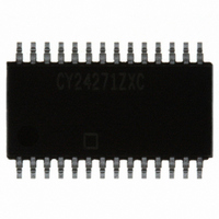
CY24271ZXC Cypress Semiconductor Corp, CY24271ZXC Datasheet

CY24271ZXC
Specifications of CY24271ZXC
CY24271ZXC
Available stocks
Related parts for CY24271ZXC
CY24271ZXC Summary of contents
Page 1
... MHz offset ❐ 100 or 133 MHz differential clock input ■ Logic Block Diagram Cypress Semiconductor Corporation Document Number: 001-00411 Rev. *C Rambus XDR™ Clock Generator 300–800 MHz high speed clock support ■ ...
Page 2
Contents Pinouts .............................................................................. 3 PLL Multiplier .................................................................... 4 Device ID and SMBus Device Address ........................... 4 Modes of Operation .......................................................... 4 SMBus Protocol ................................................................ 5 Input Clock Signal ............................................................ 5 SMBus Data Byte Definitions .......................................... 5 Absolute Maximum Conditions ....................................... ...
Page 3
Pinouts Figure 1. Pin Diagram - 28-pin TSSOP Table 1. Pin Definitions - 28-pin TSSOP Pin No. Name IO 1 VDDP PWR 2 VSSP GND 3 ISET I 4 VSS GND 5 REFCLK I 6 REFCLKB I 7 VDDC PWR ...
Page 4
PLL Multiplier Table shows the frequency multipliers in the PLL, selectable by programming the SMBus registers MULT0, MULT1, and MULT2. Default multiplier at power Table 2. PLL Multiplier Selection Register Frequency Multiplier MULT2 MULT1 MULT0 0 0 ...
Page 5
Table 4. Modes of Operation for CY24271 EN /BYPASS RegTest RegA RegB RegC RegD CLK0/CLK0B ...
Page 6
Table 5. Command Code 80h Bit Register POD 7 Reserved 0 6 MULT2 0 5 MULT1 0 4 MULT0 1 3 RegA 1 2 RegB 1 1 RegC 1 0 RegD 1 [6] Table 6. Command Code 81h Bit ...
Page 7
Figure 2. Differential and Single-Ended Clock Inputs REFCLKB Input REFCLK XDR Clock Generator Differential Input Absolute Maximum Conditions Parameter Description V Clock Buffer Supply Voltage DD V Core Supply Voltage DDC V PLL Supply Voltage DDP V Input Voltage (SCL ...
Page 8
DC Operating Conditions Parameter Description V Supply Voltage for PLL DDP V Supply Voltage for Core DDC V Supply Voltage for Clock Buffers DD V Input High Voltage, REFCLK/REFCLKB IHCLK V Input Low Voltage, REFCLK/REFCLKB ILCLK [7] V Crossing Point ...
Page 9
AC Operating Conditions [10] The AC operating conditions follow. Parameter Description t REFCLK, REFCLKB input cycle time CYCLE,IN [11] t Input Cycle to Cycle Jitter JIT,IN(cc) [12] t Input Duty Cycle DCIN Rise and Fall Times RIN ...
Page 10
AC Electrical Specification [21] The AC Electrical specifications follow. Parameter [22] t Clock Cycle time CYCLE t Jitter over 1-6 clock cycles at 400–635 MHz JIT(cc) Jitter over 1-6 clock cycles at 638–800 MHz L Phase noise SSB spectral purity ...
Page 11
Example External Resistor Values and Termination Voltages for a 50 Channel Parameter Value 200 1.2V T Signal Waveforms A physical signal ...
Page 12
CLK CLKB t CYCLE CYCLE,i CLK CLKB t PW- t CYCLE, t DC,ERR Document Number: 001-00411 Rev. *C Figure 6. Cycle-to-cycle Jitter t CYCLE,i CYCLE,i+1 over 10,000 consecutive cycles Figure 7. Cycle-to-cycle Duty-cycle Error ...
Page 13
... Ordering Information Part Number Pb-free CY24271ZXC CY24271ZXCT Ordering Code Definitions CY 24721 Package Drawing and Dimension Figure 8. 28-pin Thin Shrunk Small Outline Package (4.40-mm Body) Z29 Document Number: 001-00411 Rev. *C Package Type 28-pin TSSOP 28-pin TSSOP – Tape and Reel T = Tape and Reel ...
Page 14
Acronyms Acronym Description CMOS complementary metal oxide semiconductor ESD electrostatic discharge PLL phase locked loop TSSOP thin shrunk small outline package XDR extended data rate Document Conventions Units of Measure Symbol Unit of Measure °C degree Celsius Hz Hertz kHz ...
Page 15
Document History Page Document Title: CY24271 Rambus XDR™ Clock Generator Document Number: 001-00411 Orig. of REV. ECN NO. Issue Date Change ** 378263 See ECN RGL *A 492065 See ECN KKVTMP 1) New Pin definition table *B 1333483 See ...
Page 16
... Cypress against all charges. Any Source Code (software and/or firmware) is owned by Cypress Semiconductor Corporation (Cypress) and is protected by and subject to worldwide patent protection (United States and foreign), United States copyright laws and international treaty provisions. Cypress hereby grants to licensee a personal, non-exclusive, non-transferable license to copy, use, modify, create derivative works of, and compile the Cypress Source Code and derivative works for the sole purpose of creating custom software and or firmware in support of licensee product to be used only in conjunction with a Cypress integrated circuit as specified in the applicable agreement ...


