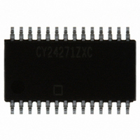
CY24271ZXC Cypress Semiconductor Corp, CY24271ZXC Datasheet - Page 5

CY24271ZXC
Manufacturer Part Number
CY24271ZXC
Description
IC CLOCK GEN XDR 28-TSSOP
Manufacturer
Cypress Semiconductor Corp
Type
Clock Generator, Fanout Distributionr
Series
Rambus™, XDR™r
Datasheet
1.CY24271ZXC.pdf
(16 pages)
Specifications of CY24271ZXC
Number Of Circuits
1
Package / Case
28-TSSOP
Pll
Yes with Bypass
Input
Clock
Output
Clock
Ratio - Input:output
1:4
Differential - Input:output
Yes/Yes
Frequency - Max
1.067MHz
Divider/multiplier
No/Yes
Voltage - Supply
2.375 V ~ 2.625 V
Operating Temperature
0°C ~ 70°C
Mounting Type
Surface Mount
Frequency-max
800MHz
Minimum Input Frequency
133 MHz, 100 MHz
Output Frequency Range
300 MHz to 800 MHz
Supply Voltage (max)
2.625 V
Supply Voltage (min)
2.375 V
Maximum Operating Temperature
+ 70 C
Minimum Operating Temperature
0 C
Mounting Style
SMD/SMT
Operating Supply Voltage
2.5 V
Lead Free Status / RoHS Status
Lead free / RoHS Compliant
Lead Free Status / RoHS Status
Lead free / RoHS Compliant, Lead free / RoHS Compliant
Other names
428-2218-5
CY24271ZXC
CY24271ZXC
Available stocks
Company
Part Number
Manufacturer
Quantity
Price
Company:
Part Number:
CY24271ZXC
Manufacturer:
Maxim
Quantity:
12
Table 4. Modes of Operation for CY24271
SMBus Protocol
The CY24271 is a slave receiver supporting operations in the
word and byte modes described in sections 5.5.4 and 5.5.5 of
the SMBus Specification 2.0.
DC specifications are modified to RAMBUS standard to support
1.8, 2.5, and 3.3 volt devices. Time-out detection and packet
error protocol SMBus features are not supported.
Input Clock Signal
The XCG receives either a differential (REFCLK/REFCLKB) or a
single-ended reference clocking input (REFCLK).
When the reference input clock is from a different clock source,
it must meet the voltage levels and timing requirements listed in
DC Operating Conditions on page 8
Conditions on page
Document Number: 001-00411 Rev. *C
Notes
4. Bypass Mode: REFCLK bypasses the PLL to the output drivers.
5. Default mode of operation is at power up.
EN
H
H
H
H
H
H
H
H
H
H
H
H
H
H
H
H
H
H
L
/BYPASS RegTest RegA RegB RegC RegD CLK0/CLK0B
H
H
H
H
H
H
H
H
H
H
H
H
H
H
H
H
X
X
L
9.
0
X
1
0
0
0
0
0
0
0
0
0
0
0
0
0
0
0
0
[5]
1
X
X
X
0
0
0
0
0
0
0
0
1
1
1
1
1
1
1
[5]
1
X
X
X
0
0
0
0
1
1
1
1
0
0
0
0
1
1
1
[5]
and
1
AC Operating
X
X
X
0
0
1
1
0
0
1
1
0
0
1
1
0
0
1
[5]
1
X
X
X
0
1
0
1
0
1
0
1
0
1
0
1
0
1
0
[5]
REFCLKB
CLK/CLKB
CLK/CLKB
CLK/CLKB
CLK/CLKB
CLK/CLKB
CLK/CLKB
CLK/CLKB
CLK/CLKB
REFCLK/
High Z
High Z
High Z
High Z
High Z
High Z
High Z
High Z
High Z
For a single-ended clock input, an external voltage divider and a
supply voltage, as shown in
voltage V
point of REFCLK. For the range of V
Conditions on page
Operating Conditions tables.
SMBus Data Byte Definitions
Three data bytes are defined for the CY24271. Byte 0 is for
programming the PLL multiplier registers and clock output
registers.
The definition of Byte 2 is shown in
on page
revision numbers of the device and the lower three bits are the
ID numbers assigned to the vendor by Rambus.
[4]
TH
6, and
CLK1/CLK1B CLK2/CLK2B CLK3/CLK3B
at the REFCLKB pin. This determines the proper trip
CLK/CLKB
CLK/CLKB
CLK/CLKB
CLK/CLKB
CLK/CLKB
CLK/CLKB
CLK/CLKB
CLK/CLKB
REFCLKB
Reserved for Vendor Test
REFCLK/
High Z
High Z
High Z
High Z
High Z
High Z
High Z
High Z
High Z
Table 7 on page
8, the outputs also meet the DC and AC
CLK/CLKB
CLK/CLKB
CLK/CLKB
CLK/CLKB
CLK/CLKB
CLK/CLKB
CLK/CLKB
CLK/CLKB
REFCLKB
REFCLK/
High Z
High Z
High Z
High Z
High Z
High Z
High Z
High Z
High Z
Figure
6. The upper five bits are the
TH
Table 5 on page
specified in
2, provide a reference
CLK/CLKB
CLK/CLKB
CLK/CLKB
CLK/CLKB
CLK/CLKB
CLK/CLKB
CLK/CLKB
CLK/CLKB
REFCLKB
REFCLK/
High Z
High Z
High Z
High Z
High Z
High Z
High Z
High Z
High Z
CY24271
DC Operating
Page 5 of 16
6,
Table 6
[+] Feedback


