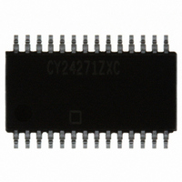
CY24271ZXC Cypress Semiconductor Corp, CY24271ZXC Datasheet - Page 9

CY24271ZXC
Manufacturer Part Number
CY24271ZXC
Description
IC CLOCK GEN XDR 28-TSSOP
Manufacturer
Cypress Semiconductor Corp
Type
Clock Generator, Fanout Distributionr
Series
Rambus™, XDR™r
Datasheet
1.CY24271ZXC.pdf
(16 pages)
Specifications of CY24271ZXC
Number Of Circuits
1
Package / Case
28-TSSOP
Pll
Yes with Bypass
Input
Clock
Output
Clock
Ratio - Input:output
1:4
Differential - Input:output
Yes/Yes
Frequency - Max
1.067MHz
Divider/multiplier
No/Yes
Voltage - Supply
2.375 V ~ 2.625 V
Operating Temperature
0°C ~ 70°C
Mounting Type
Surface Mount
Frequency-max
800MHz
Minimum Input Frequency
133 MHz, 100 MHz
Output Frequency Range
300 MHz to 800 MHz
Supply Voltage (max)
2.625 V
Supply Voltage (min)
2.375 V
Maximum Operating Temperature
+ 70 C
Minimum Operating Temperature
0 C
Mounting Style
SMD/SMT
Operating Supply Voltage
2.5 V
Lead Free Status / RoHS Status
Lead free / RoHS Compliant
Lead Free Status / RoHS Status
Lead free / RoHS Compliant, Lead free / RoHS Compliant
Other names
428-2218-5
CY24271ZXC
CY24271ZXC
Available stocks
Company
Part Number
Manufacturer
Quantity
Price
Company:
Part Number:
CY24271ZXC
Manufacturer:
Maxim
Quantity:
12
AC Operating Conditions
The AC operating conditions follow.
DC Electrical Specifications
Document Number: 001-00411 Rev. *C
Notes
t
t
t
t
t
p
f
t
C
C
f
V
V
V
V
I
I
I
I
I
V
I
I
Z
10. Not 100% tested except V
11. Jitter measured at crossing points and is the absolute value of the worst case deviation.
12. Measured at crossing points.
13. If input modulation is used; input modulation is allowed but not required.
14. The amount of allowed spreading for any non-triangular modulation is determined by the induced downstream tracking skew that cannot exceed the skew generated
15. V
16. V
17. V
18. I
CYCLE,IN
JIT,IN(cc)
DCIN
RIN
MIN
SR,IN
SCL
DD
DD
DD
OL/
OL,ABS
OL,SDA
OZ
19. Minimum I
20. Z
Parameter
Parameter
MIN
OX
COS
OL,ABS
ISET
OL,SDA
OUT
IN,REF
IN,CMOS
RIN
[10]
[10]
[10]
by the specified 0.6% triangular modulation. Typically, the amount of allowed non-triangular modulation is about 0.5%.
I
[13]
REF
[10]
REF
/ t
OUT
[13]
OX
COS
OL_ABS
[12]
[10]
/ t
FIN
is measured on external divider network.
is equal to V
FIN
is defined at the output pins as (0.94 V – 0.90 V)/(I
= (clock output high voltage – clock output low voltage), measured on the external divider network.
is measured at the clock output pins of the package.
OL,ABS
REFCLK, REFCLKB input cycle time
Input Cycle to Cycle Jitter
Input Duty Cycle
Rise and Fall Times
Rise and Fall Times Difference
Modulation Index for triangular modulation
Modulation Index for non-triangular modulation
Input Frequency Modulation
Input Slew Rate (measured at 20%–80% of
input voltage) for REFCLK
Capacitance at REFCLK inputs
Capacitance at CMOS inputs
SMBus clock frequency input in SCL pin
Differential output crossing point voltage
Output voltage swing (peak-to-peak single-ended)
Absolute output low voltage at CLK[3:0], CLK[3:0]B
Reference voltage for swing controlled current, I
Power Supply Current at 2.625 V, f
Power Supply Current at 2.625 V, f
Power Supply Current at 2.625 V, f
Ratio of output low current to reference current
Minimum current at V
SDA output low voltage at test condition of SDA output low current = 4 mA
SDA output low voltage at test condition of SDA voltage = 0.8 V
Current during High Z per pin at CLK[3:0], CLK[3:0]B
Output dynamic impedance when clock output signal is at V
ISET
is measured at the clock output pin with R
/R
RC
IXCLK
.
and V
Description
IXCLK
[10]
OL,ABS
. Parameters guaranteed by design and characterizations, not 100% tested in production.
[11]
[19]
Description
0.94
ref
ref
ref
RC
– I
= 100 MHz, and f
= 133 MHz, and f
= 133 MHz, and f
= 148 ohms or less.
0.90
[15]
) under conditions specified for I
[18]
REF
REFSEL = 0, /BYPASS = High
REFSEL = 1, /BYPASS = High
/BYPASS = Low
Over 10,000 cycles
Measured at 20%–80% of input
voltage for REFCLK and
REFCLKB inputs
[16]
[17]
out
out
out
= 300 MHz
= 667 MHz
= 800 MHz
OL
Condition
= 0.9 V
OL, ABS
[20]
.
1000
0.85
0.98
Min
300
0.9
6.8
45
–
–
–
–
6
–
40%
Min
Typ
325
175
DC
1.0
1.0
7.0
30
9
7
4
–
–
–
–
1
–
–
–
–
–
–
–
–
–
–
–
0.5
Max
1.02
60%
Max
350
125
130
185
700
150
100
1.1
7.2
0.4
0.6
85
10
11
33
10
–
–
–
–
8
–
4
7
[14]
CY24271
t
CYCLE
Unit
V/ns
Unit
mV
mA
mA
mA
mA
mA
kHz
kHz
Page 9 of 16
A
pF
pF
ns
ns
ns
ps
ps
ps
V
V
V
V
%
%
[+] Feedback


