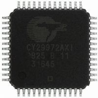
CY29972AXI Cypress Semiconductor Corp, CY29972AXI Datasheet - Page 4

CY29972AXI
Manufacturer Part Number
CY29972AXI
Description
IC CLK ZDB 12OUT 125MHZ 52TQFP
Manufacturer
Cypress Semiconductor Corp
Type
Fanout Distribution, Multiplexer , Spread Spectrum Clock Generator, Zero Delay Bufferr
Datasheet
1.CY29972AXI.pdf
(8 pages)
Specifications of CY29972AXI
Number Of Circuits
1
Package / Case
52-TQFP
Pll
Yes with Bypass
Input
Clock, Crystal
Output
Clock
Ratio - Input:output
4:12
Differential - Input:output
No/No
Frequency - Max
125MHz
Divider/multiplier
Yes/No
Voltage - Supply
2.9 V ~ 3.6 V
Operating Temperature
-40°C ~ 85°C
Mounting Type
Surface Mount
Frequency-max
125MHz
Maximum Input Frequency
480 MHz
Minimum Input Frequency
200 MHz
Output Frequency Range
125 MHz
Supply Voltage (max)
3.6 V
Supply Voltage (min)
2.9 V
Maximum Operating Temperature
+ 85 C
Minimum Operating Temperature
- 40 C
Mounting Style
SMD/SMT
Operating Supply Voltage
3.3 V
Lead Free Status / RoHS Status
Lead free / RoHS Compliant
Lead Free Status / RoHS Status
Lead free / RoHS Compliant, Lead free / RoHS Compliant
Other names
428-2236
CY29972AXI
CY29972AXI
Available stocks
Company
Part Number
Manufacturer
Quantity
Price
Company:
Part Number:
CY29972AXI
Manufacturer:
CY
Quantity:
4 918
Company:
Part Number:
CY29972AXI
Manufacturer:
Cypress Semiconductor Corp
Quantity:
10 000
Company:
Part Number:
CY29972AXIT
Manufacturer:
Cypress Semiconductor Corp
Quantity:
10 000
Part Number:
CY29972AXIT
Manufacturer:
CYPRESS
Quantity:
20 000
Document #: 38-07290 Rev. *C
SYNC Output
In situations where output frequency relationships are not
integer multiples of each other, the SYNC output provides a
signal for system synchronization. The CY29972 monitors the
relationship between the QA and QC output clocks. It provides
a LOW-going pulse, one period in duration, one period prior to
the coincident rising edges of the QA and QC outputs. The
SYNC
SYNC
SYNC
SYNC
SYNC
SYNC
SYNC
VCO
QC
QC
QC
QC
QC
QC
QC
QA
QA
QA
QA
QA
QA
QA
Figure 1. Timing Diagram
duration and placement of the pulse depend on the higher of
the QA and QC output frequencies. The following timing
diagram illustrates various waveforms for the SYNC output.
Note that the SYNC output is defined for all possible combina-
tions of QA and QC outputs, even though under some relation-
ships the lower frequency clock could be used as a synchro-
nizing signal.
1:1 Mode
2:1 Mode
3:1 Mode
3:2 Mode
4:1 Mode
4:3 Mode
6:1 Mode
CY29972
Page 4 of 8
[+] Feedback


