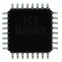
ICS84320AY-01LN IDT, Integrated Device Technology Inc, ICS84320AY-01LN Datasheet - Page 14

ICS84320AY-01LN
Manufacturer Part Number
ICS84320AY-01LN
Description
IC SYNTHESIZER GP LVPECL 32-LQFP
Manufacturer
IDT, Integrated Device Technology Inc
Series
HiPerClockS™r
Type
Frequency Synthesizerr
Datasheet
1.ICS84320AY-01LN.pdf
(22 pages)
Specifications of ICS84320AY-01LN
Pll
Yes with Bypass
Input
Crystal
Output
LVPECL
Number Of Circuits
1
Ratio - Input:output
1:2
Differential - Input:output
No/Yes
Frequency - Max
780MHz
Divider/multiplier
Yes/No
Voltage - Supply
3.135 V ~ 3.465 V
Operating Temperature
0°C ~ 70°C
Mounting Type
Surface Mount
Package / Case
32-LQFP
Frequency-max
780MHz
Number Of Elements
1
Supply Current
155mA
Pll Input Freq (min)
14MHz
Pll Input Freq (max)
40MHz
Operating Supply Voltage (typ)
3.3V
Operating Temp Range
0C to 70C
Package Type
TQFP
Output Frequency Range
77.5 to 780MHz
Operating Supply Voltage (min)
2.915/3.135V
Operating Supply Voltage (max)
3.465V
Operating Temperature Classification
Commercial
Pin Count
32
Lead Free Status / RoHS Status
Lead free / RoHS Compliant
Other names
800-1140
84320AY-01LN
84320AY-01LN
Available stocks
Company
Part Number
Manufacturer
Quantity
Price
Company:
Part Number:
ICS84320AY-01LN
Manufacturer:
IDT, Integrated Device Technology Inc
Quantity:
10 000
Part Number:
ICS84320AY-01LN
Manufacturer:
ICS
Quantity:
20 000
Company:
Part Number:
ICS84320AY-01LNT
Manufacturer:
IDT, Integrated Device Technology Inc
Quantity:
10 000
VFQFN EPAD T
In order to maximize both the removal of heat from the package
and the electrical performance, a land pattern must be
incorporated on the Printed Circuit Board (PCB) within the
footprint of the package corresponding to the exposed metal
pad or exposed heat slug on the package, as shown in Figure
7. The solderable area on the PCB, as defined by the solder
mask, should be at least the same size/shape as the exposed
pad/slug area on the package to maximize the thermal/
electrical performance. Sufficient clearance should be
designed on the PCB between the outer edges of the land
pattern and the inner edges of pad pattern for the leads to
avoid any shorts.
While the land pattern on the PCB provides a means of heat
transfer and electrical grounding from the package to the board
through a solder joint, thermal vias are necessary to effectively
conduct from the surface of the PCB to the ground plane(s).
The land pattern must be connected to ground through these
vias. The vias act as “heat pipes”. The number of vias (i.e.
84320AY-01
F
IGURE
PIN PAD
HERMAL
PIN
7. P.C.A
R
ELEASE
SSEMBLY FOR
SOLDER
GROUND PLANE
P
ATH
E
XPOSED
P
AD
EXPOSED HEAT SLUG
T
THERMAL VIA
www.idt.com
HERMAL
14
“heat pipes”) are application specific and dependent upon
the package power dissipation as well as electrical
conductivity requirements. Thus, thermal and electrical
analysis and/or testing are recommended to determine the
minimum number needed. Maximum thermal and electrical
performance is achieved when an array of vias is incorporated
in the land pattern. It is recommended to use as many vias
connected to ground as possible. It is also recommended that
the via diameter should be 12 to 13mils (0.30 to 0.33mm) with
1oz copper via barrel plating. This is desirable to avoid any
solder wicking inside the via during the soldering process
which may result in voids in solder between the exposed
pad/slug and the thermal land. Precautions should be taken
to eliminate any solder voids between the exposed heat slug
and the land pattern. Note: These recommendations are to be
used as a guideline only. For further information, refer to the
Application Note on the Surface Mount Assembly of Amkor’s
Thermally/Electrically Enhance Leadfame Base Package,
Amkor Technology.
R
780MH
ELEASE
P
ATH
LVPECL F
Z
–S
, C
LAND PATTERN
(GROUND PAD)
IDE
RYSTAL
V
SOLDER
IEW
(D
REQUENCY
-
RAWING NOT TO
TO
-3.3V D
ICS84320-01
PIN
S
S
PIN PAD
CALE
IFFERENTIAL
YNTHESIZER
REV. D JULY 26, 2010
)


