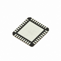
SI5317D-C-GM Silicon Laboratories Inc, SI5317D-C-GM Datasheet - Page 23

SI5317D-C-GM
Manufacturer Part Number
SI5317D-C-GM
Description
IC CLK JITTER CLEANR PROG 36QFN
Manufacturer
Silicon Laboratories Inc
Type
Jitter Cleanerr
Series
Si5317r
Datasheet
1.SI5317C-C-GM.pdf
(46 pages)
Specifications of SI5317D-C-GM
Package / Case
36-QFN
Pll
Yes with Bypass
Input
Clock, Crystal
Output
CML, CMOS, LVDS, LVPECL
Number Of Circuits
1
Ratio - Input:output
1:2
Differential - Input:output
Yes/Yes
Frequency - Max
100MHz
Divider/multiplier
No/No
Voltage - Supply
1.71 V ~ 3.63 V
Operating Temperature
-40°C ~ 85°C
Mounting Type
Surface Mount
Frequency-max
100MHz
Termination Style
SMD/SMT
Output Format
CML
Dimensions
5 mm W x 7 mm L x 1.85 mm H
Minimum Operating Temperature
- 40 C
Maximum Operating Temperature
+ 85 C
Mounting Style
SMD/SMT
Product
XO
Frequency
10 MHz to 945 MHz
Frequency Stability
+/- 20 PPM
Supply Voltage
3.3 Volts
Height
1.85 mm
Lead Free Status / RoHS Status
Lead free / RoHS Compliant
Lead Free Status / RoHS Status
Lead free / RoHS Compliant, Lead free / RoHS Compliant
Other names
336-1920
3.4. Alarms
Summary alarms are available to indicate the overall status of the input signals. Alarm outputs stay high until all
the alarm conditions for that alarm output are cleared.
3.4.1. Loss-of-Signal
The device has loss-of-signal circuitry that continuously monitors CKIN for missing pulses.
An LOS condition on CKIN causes the LOS alarm to become active. Once a LOS alarm is asserted, it remains
asserted until the input clock is validated over a designated time period. The time to clear LOS after a valid input
clock appears is listed in Table 4, “AC Characteristics”. If another error condition on the same input clock is
detected during the validation time, then the alarm remains asserted and the validation time starts over.
3.4.1.1. LOS Algorithm
The LOS circuitry divides down each input clock to produce an 8 kHz to 2 MHz signal. The LOS circuitry
oversamples this divided down input clock using a 40 MHz clock to search for extended periods of time without
input clock transitions. If the LOS monitor detects twice the normal number of samples without a clock edge, a
LOS alarm is declared. Table 4, “AC Characteristics” gives the minimum and maximum amount of time for the
LOS monitor to trigger.
3.4.1.2. Lock Detect
The PLL lock detection algorithm indicates the lock status on the LOL output pin. The algorithm works by
continuously monitoring the phase of the input clock in relation to the phase of the feedback clock. If the time
between two consecutive phase cycle slips is greater than the retrigger time, the PLL is in lock. The LOL output
has a guaranteed minimum pulse width as shown in Table 4, “AC Characteristics”. The LOL pin is also held in the
active state during an internal PLL calibration. The retrigger time is automatically set based on the PLL closed loop
bandwidth (see Table 10).
3.5. VCO Freeze
The Si5317 device features a VCO freeze mode whereby the DSPLL is locked to a frequency value.
If an LOS condition exists on the selected input clock, the device freezes the VCO. In this mode, the device
provides a stable output frequency until the input clock returns and is validated. When the device enters VCO
freeze, the internal oscillator is initially held to its last frequency value.
3.5.1. Recovery from VCO Freeze
When the input clock signal returns, the device transitions from VCO freeze to the selected input clock.
PLL Bandwidth Setting (BW)
Table 10. Lock Detect Retrigger Time
1920–3840 Hz
3840–7680 Hz
960–1920 Hz
120–240 Hz
240–480 Hz
480–960 Hz
60–120 Hz
Rev. 1.1
Retrigger Time (ms)
0.833
26.5
13.3
1.66
6.6
3.3
53
Si5317
23


