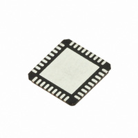
SI5317D-C-GM Silicon Laboratories Inc, SI5317D-C-GM Datasheet - Page 27

SI5317D-C-GM
Manufacturer Part Number
SI5317D-C-GM
Description
IC CLK JITTER CLEANR PROG 36QFN
Manufacturer
Silicon Laboratories Inc
Type
Jitter Cleanerr
Series
Si5317r
Datasheet
1.SI5317C-C-GM.pdf
(46 pages)
Specifications of SI5317D-C-GM
Package / Case
36-QFN
Pll
Yes with Bypass
Input
Clock, Crystal
Output
CML, CMOS, LVDS, LVPECL
Number Of Circuits
1
Ratio - Input:output
1:2
Differential - Input:output
Yes/Yes
Frequency - Max
100MHz
Divider/multiplier
No/No
Voltage - Supply
1.71 V ~ 3.63 V
Operating Temperature
-40°C ~ 85°C
Mounting Type
Surface Mount
Frequency-max
100MHz
Termination Style
SMD/SMT
Output Format
CML
Dimensions
5 mm W x 7 mm L x 1.85 mm H
Minimum Operating Temperature
- 40 C
Maximum Operating Temperature
+ 85 C
Mounting Style
SMD/SMT
Product
XO
Frequency
10 MHz to 945 MHz
Frequency Stability
+/- 20 PPM
Supply Voltage
3.3 Volts
Height
1.85 mm
Lead Free Status / RoHS Status
Lead free / RoHS Compliant
Lead Free Status / RoHS Status
Lead free / RoHS Compliant, Lead free / RoHS Compliant
Other names
336-1920
4.2. Output Clock Driver
The Si5317 has a flexible output driver structure that can drive a variety of loads, including LVPECL, LVDS, CML,
and CMOS formats. The signal format is selected for CKOUT output using the SFOUT [1:0] pins. This modifies the
output common mode and differential signal swing. See Table 2, “DC Characteristics” for output driver
specifications. The SFOUT [1:0] pins are three-level input pins with the states designated as L (ground), M (V
and H (V
When SFOUT = LH for CMOS, bypass mode is not supported.
For the CMOS setting (SFOUT = LH), both output pins drive single-ended in-phase signals and should be
externally shorted together to obtain the drive strength specified in Table 2, “DC Characteristics”.
DD
Figure 12. Typical CMOS Output Circuit (Tie CKOUTn+ and CKOUTn– Together)
). Table 12 shows the signal formats based on the supply voltage and the type of load being driven.
CKOUTn
Si5317
Table 12. Output Signal Format Selection (SFOUT)
Figure 11. Typical Differential Output Circuit
Z0 = 50
SFOUT[1:0]
Z0 = 50
All Others
CKOUTn
HM
MH
HL
LH
LM
ML
Si5317
Outputs Together for Greater Strength
Rev. 1.1
Low-swing LVDS
Optionally Tie CKOUTn
Signal Format
Reserved
Disabled
LVPECL
CMOS
LVDS
CML
CMOS
Logic
100
Rcvr
Si5317
DD
/2),
27


