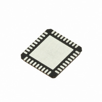
SI5317D-C-GM Silicon Laboratories Inc, SI5317D-C-GM Datasheet - Page 45

SI5317D-C-GM
Manufacturer Part Number
SI5317D-C-GM
Description
IC CLK JITTER CLEANR PROG 36QFN
Manufacturer
Silicon Laboratories Inc
Type
Jitter Cleanerr
Series
Si5317r
Datasheet
1.SI5317C-C-GM.pdf
(46 pages)
Specifications of SI5317D-C-GM
Package / Case
36-QFN
Pll
Yes with Bypass
Input
Clock, Crystal
Output
CML, CMOS, LVDS, LVPECL
Number Of Circuits
1
Ratio - Input:output
1:2
Differential - Input:output
Yes/Yes
Frequency - Max
100MHz
Divider/multiplier
No/No
Voltage - Supply
1.71 V ~ 3.63 V
Operating Temperature
-40°C ~ 85°C
Mounting Type
Surface Mount
Frequency-max
100MHz
Termination Style
SMD/SMT
Output Format
CML
Dimensions
5 mm W x 7 mm L x 1.85 mm H
Minimum Operating Temperature
- 40 C
Maximum Operating Temperature
+ 85 C
Mounting Style
SMD/SMT
Product
XO
Frequency
10 MHz to 945 MHz
Frequency Stability
+/- 20 PPM
Supply Voltage
3.3 Volts
Height
1.85 mm
Lead Free Status / RoHS Status
Lead free / RoHS Compliant
Lead Free Status / RoHS Status
Lead free / RoHS Compliant, Lead free / RoHS Compliant
Other names
336-1920
D
Revision 0.1 to Revision 0.15
Revision 0.15 to Revision 0.2
Revision 0.2 to Revision 1.0
Revision 1.0 to Revision 1.1
Material
Material
OCUMENT
Updated corresponding sections and pinouts to add
CKOUT2, INC/DEC, and DBL2_BY functionality.
Updated functional block diagram on page 1.
Updated Table 2 IDD (DD is subscript).
Added Differential Rise/Fall Time spec to Table 2.
Updated pin assignment symbol and pin description
on page 1 and in section 9 to add CKOUT2,
INC/DEC, and DBL2_BY.
Added section 3.6. "PLL Bypass Mode”.
Updated section 8 diagram to add CKOUT2 and
DBL2_BY.
Added additional CMOS Termination with
attenuation figure.
Corrected pin name assignment (pin28) diagram on
page 1 and section 9, page 35 to match pin
description name.
Updated all the frequency plans in Table 8 to provide
coverage over the entire frequency range.
Updated bypass mode, ESD specifications and
absolute max V
Corrected INC/DEC pinout.
Removed Output Short to GNDon page 5.
Removed duplicate lock time specification on page
11.
Removed Time to Clear LOS alarm on page 11.
Revised spurious noise values.
Revised phase noise values.
Increased the maximum input/output frequency to
711 MHz
Added reference to “AN591: Crystal Selection for the
Si5315 and Si5317”
C
DD
HANGE
.
L
IST
Rev. 1.1
Si5317
45


