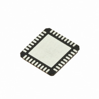
SI5317D-C-GM Silicon Laboratories Inc, SI5317D-C-GM Datasheet - Page 38

SI5317D-C-GM
Manufacturer Part Number
SI5317D-C-GM
Description
IC CLK JITTER CLEANR PROG 36QFN
Manufacturer
Silicon Laboratories Inc
Type
Jitter Cleanerr
Series
Si5317r
Datasheet
1.SI5317C-C-GM.pdf
(46 pages)
Specifications of SI5317D-C-GM
Package / Case
36-QFN
Pll
Yes with Bypass
Input
Clock, Crystal
Output
CML, CMOS, LVDS, LVPECL
Number Of Circuits
1
Ratio - Input:output
1:2
Differential - Input:output
Yes/Yes
Frequency - Max
100MHz
Divider/multiplier
No/No
Voltage - Supply
1.71 V ~ 3.63 V
Operating Temperature
-40°C ~ 85°C
Mounting Type
Surface Mount
Frequency-max
100MHz
Termination Style
SMD/SMT
Output Format
CML
Dimensions
5 mm W x 7 mm L x 1.85 mm H
Minimum Operating Temperature
- 40 C
Maximum Operating Temperature
+ 85 C
Mounting Style
SMD/SMT
Product
XO
Frequency
10 MHz to 945 MHz
Frequency Stability
+/- 20 PPM
Supply Voltage
3.3 Volts
Height
1.85 mm
Lead Free Status / RoHS Status
Lead free / RoHS Compliant
Lead Free Status / RoHS Status
Lead free / RoHS Compliant, Lead free / RoHS Compliant
Other names
336-1920
Si5317
38
Pin #
23
22
27
26
25
24
29
28
33
30
34
35
CKOUT1–
CKOUT1+
CKOUT2–
CKOUT2+
Pin Name
FRQSEL3
FRQSEL2
FRQSEL1
FRQSEL0
BWSEL1
BWSEL0
SFOUT0
SFOUT1
Table 14. Si5317 Pin Descriptions (Continued)
I/O
O
O
I
I
Signal Level
3-Level
3-Level
Multi
Multi
Loop Bandwidth Select.
Three level inputs that select the DSPLL closed loop band-
width. See Table 9 on page 22 for available settings.
These pins have both weak pull-ups and weak pull-downs
and default to M.
Some designs may require an external resistor voltage
divider when driven by an active device that will tri-state.
Frequency Select.
Three level inputs that select the input clock and clock range.
See Table 9 on page 22.
These pins have both weak pull-ups and weak pull-downs
and default to M.
Some designs may require an external resistor voltage
divider when driven by an active device that will tri-state.
Clock Output 1.
Output signal format is selected by SFOUT pins. Differential
formats supported for LVPECL, LVDS, and CML compatible
modes. For single-ended CMOS format, both output pins
drive identical, in-phase clock outputs.
Signal Format Select.
Three-level inputs that select the output signal format (com-
mon mode voltage and differential swing) for both CKOUT1
and CKOUT2.
These pins have both weak pull-ups and weak pull-downs
and default to M.
Some designs may require an external resistor voltage
divider when driven by an active device that will tri-state.*
CMOS outputs do not support bypass mode.
Clock Output 2.
Output signal format is selected by SFOUT pins. Differential
formats supported for LVPECL, LVDS, and CML compatible
modes. For single-ended CMOS format, both output pins
drive identical, in-phase clock outputs.
Rev. 1.1
SFOUT[1:0]
MM
HM
MH
HH
ML
LM
HL
LH
LL
Description
Reserved
LVDS
CML
LVPECL
Reserved
LVDS—Low Swing
CMOS
Disable
Reserved
Signal Format


