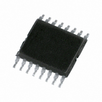
74HCT9046APW,112 NXP Semiconductors, 74HCT9046APW,112 Datasheet - Page 5

74HCT9046APW,112
Manufacturer Part Number
74HCT9046APW,112
Description
IC PLL W/BAND GAP VCO 16-TSSOP
Manufacturer
NXP Semiconductors
Type
Phase Lock Loop (PLL)r
Series
74HCTr
Datasheet
1.74HCT9046AD118.pdf
(43 pages)
Specifications of 74HCT9046APW,112
Number Of Circuits
1
Package / Case
16-TSSOP
Pll
Yes
Input
Clock
Output
Clock
Ratio - Input:output
2:2
Differential - Input:output
No/No
Frequency - Max
16MHz
Divider/multiplier
No/No
Voltage - Supply
4.5 V ~ 5.5 V
Operating Temperature
-40°C ~ 125°C
Mounting Type
Surface Mount
Frequency-max
16MHz
Supply Voltage (max)
5.5 V
Supply Voltage (min)
4.5 V
Maximum Operating Temperature
+ 125 C
Minimum Operating Temperature
- 40 C
Mounting Style
SMD/SMT
Operating Supply Voltage
4.5 V to 5.5 V
Lead Free Status / RoHS Status
Lead free / RoHS Compliant
Other names
568-2914-5
935221200112
935221200112
NXP Semiconductors
7. Pinning information
Table 2.
74HCT9046A_6
Product data sheet
Symbol
GND
PC1_OUT/PCP_OUT
COMP_IN
VCO_OUT
INH
C1A
C1B
GND
VCO_IN
DEM_OUT
R1
R2
PC2_OUT
SIG_IN
RB
V
Fig 5.
CC
Pin configuration
Pin description
7.1 Pinning
7.2 Pin description
Pin
1
2
3
4
5
6
7
8
9
10
11
12
13
14
15
16
PC1_OUT/
Description
ground (0 V) of phase comparators
phase comparator 1 output or phase comparator pulse output
comparator input
VCO output
inhibit input
capacitor C1 connection A
capacitor C1 connection B
ground (0 V) VCO
VCO input
demodulator output
resistor R1 connection
resistor R2 connection
phase comparator 2 output; current source adjustable with R
signal input
bias resistor (R
supply voltage
PCP_OUT
VCO_OUT
COMP_IN
Rev. 06 — 15 September 2009
GND
GND
C1A
C1B
INH
1
2
3
4
5
6
7
8
74HCT9046A
bias
001aae500
) connection
16
15
14
13
12
11
10
9
V
RB
SIG_IN
PC2_OUT
R2
R1
DEM_OUT
VCO_IN
CC
PLL with band gap controlled VCO
74HCT9046A
bias
© NXP B.V. 2009. All rights reserved.
5 of 43


