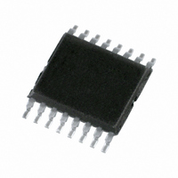
74HCT9046APW,112 NXP Semiconductors, 74HCT9046APW,112 Datasheet - Page 9

74HCT9046APW,112
Manufacturer Part Number
74HCT9046APW,112
Description
IC PLL W/BAND GAP VCO 16-TSSOP
Manufacturer
NXP Semiconductors
Type
Phase Lock Loop (PLL)r
Series
74HCTr
Datasheet
1.74HCT9046AD118.pdf
(43 pages)
Specifications of 74HCT9046APW,112
Number Of Circuits
1
Package / Case
16-TSSOP
Pll
Yes
Input
Clock
Output
Clock
Ratio - Input:output
2:2
Differential - Input:output
No/No
Frequency - Max
16MHz
Divider/multiplier
No/No
Voltage - Supply
4.5 V ~ 5.5 V
Operating Temperature
-40°C ~ 125°C
Mounting Type
Surface Mount
Frequency-max
16MHz
Supply Voltage (max)
5.5 V
Supply Voltage (min)
4.5 V
Maximum Operating Temperature
+ 125 C
Minimum Operating Temperature
- 40 C
Mounting Style
SMD/SMT
Operating Supply Voltage
4.5 V to 5.5 V
Lead Free Status / RoHS Status
Lead free / RoHS Compliant
Other names
568-2914-5
935221200112
935221200112
NXP Semiconductors
74HCT9046A_6
Product data sheet
8.3.2 Phase Comparator 2 (PC2)
This is a positive edge-triggered phase and frequency detector. When the PLL is using
this comparator, the loop is controlled by positive signal transitions and the duty cycles of
SIG_IN and COMP_IN are not important. PC2 comprises two D-type flip-flops, control
gating and a 3-state output stage with sink and source transistors acting as current
sources, henceforth called charge pump output of PC2. The circuit functions as an
up-down counter (see
count. The current switch charge pump output allows a virtually ideal performance of PC2,
due to appliance of some pulse overlap of the up and down signals, see
The pump current I
band gap reference of 2.5 V.
Where R
The current and voltage transfer function of PC2 are shown in
The phase comparator gain is:
I
K
cp
Fig 7.
P
=
=
17
--------- - A r
I
2
cp
bias
Typical waveforms for PLL using phase comparator 1; loop-locked at f
----------- - A
R
2.5
bias
is the external bias resistor between pin RB and ground.
cp
Rev. 06 — 15 September 2009
VCO_OUT
PC1_OUT
is independent from the supply voltage and is set by the internal
COMP_IN
VCO_IN
Figure
SIGN_IN
V
V
C1A
C1B
4) where SIG_IN causes an up-count and COMP_IN a down
PLL with band gap controlled VCO
74HCT9046A
Figure
mbd100
GND
V
C1A
C1B
CC
9.
© NXP B.V. 2009. All rights reserved.
Figure
0
8a.
9 of 43


