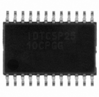
IDTCSP2510CPGG IDT, Integrated Device Technology Inc, IDTCSP2510CPGG Datasheet - Page 6

IDTCSP2510CPGG
Manufacturer Part Number
IDTCSP2510CPGG
Description
IC CLK DVR ZD BUFFER PLL 24TSSOP
Manufacturer
IDT, Integrated Device Technology Inc
Type
PLL Driver, Zero Delay Bufferr
Datasheet
1.IDTCSP2510CPG8.pdf
(9 pages)
Specifications of IDTCSP2510CPGG
Pll
Yes with Bypass
Input
Clock
Output
Clock
Number Of Circuits
1
Ratio - Input:output
1:10
Differential - Input:output
No/No
Frequency - Max
140MHz
Divider/multiplier
No/No
Voltage - Supply
3 V ~ 3.6 V
Operating Temperature
0°C ~ 85°C
Mounting Type
Surface Mount
Package / Case
24-TSSOP
Frequency-max
140MHz
Lead Free Status / RoHS Status
Lead free / RoHS Compliant
Other names
800-1706
800-1706-5
800-1706
CSP2510CPGG
800-1706-5
800-1706
CSP2510CPGG
Available stocks
Company
Part Number
Manufacturer
Quantity
Price
Company:
Part Number:
IDTCSP2510CPGG
Manufacturer:
ATHEROS
Quantity:
6 770
Part Number:
IDTCSP2510CPGG
Manufacturer:
IDT
Quantity:
20 000
PARAMETER MEASUREMENT INFORMATION
C
NOTES:
1. All inputs pulses are supplied by generators having the following characteristics: P
2. C
3. The outputs are measured one at a time with one transition per measurement.
4. Phase error measurements require equal loading at outputs Y and F
IDTCSP2510C
3.3V PHASE-LOCK LOOP CLOCK DRIVER
F
L
includes probe and jig capacitance.
From Output
Under Test
CLK
F
CSP2510C
BIN
PCB
TRACE
F
BOUT
Y
C
L
C
=30pF
L =
30pF
(2)
(2)
Phase ERROR and Skew Calculations
500
Load Circuit and Voltage Waveforms
500
on each
Y output
Ω
Ω
BOUT
. C
F
= C
FBOUT
Any Y
Any Y
Any Y
L
RR
6
– C
Output
FBIN
FBIN
CLK
≤ 100MHz Z
Input
or
FBIN
t
PHASE ER ROR
– C
(1)
PCB
O
TRACE
= 50Ω, t
; C
FBIN
(3,4)
t
t
t
SK(o)
t
P HASE ERROR
S K(o)
R
R
≅ 6
0.4V
≤ 1.2 ns, t
2V
pF
50% V
.
DD
F
≤ 1.2 ns.
0ºC TO 85ºC TEMPERATURE RANGE
50% V
DD
t
F
3V
0V
V
2V
0.4V
V
OH
OL


