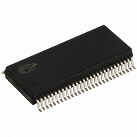
CY28329ZXC Cypress Semiconductor Corp, CY28329ZXC Datasheet

CY28329ZXC
Specifications of CY28329ZXC
Available stocks
Related parts for CY28329ZXC
CY28329ZXC Summary of contents
Page 1
... PWR PLL 2 PWR SDATA SMBus SCLK Logic Cypress Semiconductor Corporation Document #: 38-07040 Rev. *E with Differential CPU Outputs Benefits • Motherboard clock generator — Support Multiple CPUs and a chipset — Support for PCI slots and chipset — Supports AGP and Hub Link — ...
Page 2
Pin Description Name Pins REF 56 XTAL_IN 2 XTAL_OUT 3 CPU, CPU [0:3]# 44, 45, 48, 49, 51, 52, 53, 54 3V66_0 33 3V66_1/VCH 35 66IN/3V66_5 24 66BUFF [0:2] 21, 22, 23 /3V66 [2:4] PCI_F [0: PCI ...
Page 3
Function Table CPU 3V66[0:1 (MHz) MHz 100 MHz 66 MHz 1 1 133 MHz 66 MHz 0 0 100 MHz 66 MHz 0 1 133 MHz 66 MHz Mid 0 Hi-Z Hi-Z Mid 1 TCLK/2 ...
Page 4
Serial Data Interface (SMBus) To enhance the flexibility and function of the clock synthesizer, a two-signal SMBus interface is provided according to SMBus specification. Through the Serial Data Interface, various device functions such as individual clock output buffers, etc. can ...
Page 5
Data Byte 1: Bit Pin# Name Bit 7 – Bit 6 53, 54 CPU3 CPU3# Bit 5 – – Bit 4 – – Bit 3 – – Bit 2 44, 45 CPU2 CPU2# Bit 1 48, 49 CPU1 CPU1# Bit ...
Page 6
Data Byte 4: Bit Pin# Name Bit 7 – Bit 6 – Bit 5 33 3V66_0 Bit 4 35 3V66_1/VCH Bit 3 24 66IN/3V66_5 Bit 2 23 66BUFF2 Bit 1 22 66BUFF1 Bit 0 21 66BUFF0 Data Byte 5: Bit ...
Page 7
Absolute Maximum Conditions (Above which the useful life may be impaired. For user guide- lines, not tested.) Supply Voltage ..................................................–0.5 to +7.0V Input Voltage ............................................ –0. Operating Conditions over which electrical parameters are guaranteed Parameter ...
Page 8
Switching Characteristics Over the Operating Range Parameter Output t All Output Duty Cycle 1 t CPU Rise Time 2 t USB, REF, Rising Edge Rate 2 DOT t PCI, 3V66 Rising Edge Rate 2 t CPU Fall Time 3 t ...
Page 9
Definition and Application of VTTPWRGD# Signal VRM8.5 VTTPWRGD# CLOCK S0 GENERATOR S1 Document #: 38-07040 Rev. *E Vtt VTTPWRGD# BSEL0 3.3V 3.3V NPN 10K 10K CY28329 CPU BSEL1 3.3V 10K GMCH 10K Page ...
Page 10
Switching Waveforms Duty Cycle Timing (Single-Ended Output Duty Cycle Timing (CPU Differential Output All Outputs Rise/Fall Time OUTPUT t 2 CPU-CPU Clock Skew Host_b Host Host_b Host t 4 3V66-3V66 Clock Skew ...
Page 11
Switching Waveforms (continued) 3V66-PCI Clock Skew 3V66 PCI t 7 CPU Clock Cycle-Cycle Jitter Host_b Host Cycle-Cycle Clock Jitter CLK VDD and POR Timing Document #: 38-07040 Rev 1.5V VDD 1.5V POR t 10 CY28329 ...
Page 12
VTTPWRGD# Timing Diagrams GND VRM 5/12V PWR_GD VID [3:0] BSEL [1:0] VTTPWRGD FROM VRM VCC CPU CORE VTTPWRGD VCC CLOCK GEN State 0 CLOCK STATE OFF CLOCK VCO OFF CLOCK OUTPUTS GND VRM 5/12V PWRGD VID [3:0] BSEL [1:0] PWRGD ...
Page 13
PD# Assertion 66BUFF PCI PCI_F (APIC) PD# CPU CPU# 3V66 66IN USB REF PD# Deassertion 66BUFF1/GMCH 66BUFF[0:2] PCI PCI_F (APIC) PD# CPU CPU# 3V66 66IN USB REF Document #: 38-07040 Rev. *E Power Down Rest of Generator 10–30 µs min. ...
Page 14
Layout Example +3.3V Supply FB 10 µF 0.005 µ VDDQ3 1.0 - 4.7KΩ Dale ILB1206 - 300 or 2TDKACB2012L-120 or 2 Murata BLM21B601S Ceramic Caps C1 = 10–22 µ VIA ...
Page 15
... Small Shrunk Outline Package (SSOP) CY28329OXCT 56-Pin Small Shrunk Outline Package (SSOP) -Tape and Reel CY28329ZXC 56-Pin Thin Small Shrunk Outline Package (TSSOP) CY28329ZXCT 56-Pin Thin Small Shrunk Outline Package (TSSOP) Document #: 38-07040 Rev 15, 20, 31, 36, 41 14, 19,32,37, 46, 50 CY28329 ...
Page 16
... Document #: 38-07040 Rev. *E © Cypress Semiconductor Corporation, 2005. The information contained herein is subject to change without notice. Cypress Semiconductor Corporation assumes no responsibility for the use of any circuitry other than circuitry embodied in a Cypress product. Nor does it convey or imply any license under patent or other rights. Cypress products are not warranted nor intended to be used for medical, life support, life saving, critical control or safety applications, unless pursuant to an express written agreement with Cypress ...
Page 17
Document History Page Document Title: CY28329 133-MHz Spread Spectrum Clock Synthesizer/Driver with Differential CPU Outputs Document Number: 38-07040 REV. ECN NO. Issue Date ** 115133 04/26/02 *A 122733 12/14/02 *B 127128 06/13/03 *C 127899 06/26/03 *D 128179 06/27/03 *E 310457 ...


