CY28346ZXC Cypress Semiconductor Corp, CY28346ZXC Datasheet - Page 2
CY28346ZXC
Manufacturer Part Number
CY28346ZXC
Description
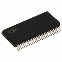
IC CLOCK SYNTHESIZER 56-TSSOP
Manufacturer
Cypress Semiconductor Corp
Type
Clock Synchronizer, Fanout Distribution, Spread Spectrum Clock Generatorr
Datasheet
1.CY28346OXC.pdf
(20 pages)
Specifications of CY28346ZXC
Pll
Yes
Input
Clock, Crystal
Output
Clock
Number Of Circuits
1
Ratio - Input:output
5:17
Differential - Input:output
No/Yes
Frequency - Max
200MHz
Divider/multiplier
Yes/No
Voltage - Supply
3.135 V ~ 3.465 V
Operating Temperature
0°C ~ 70°C
Mounting Type
Surface Mount
Package / Case
56-TSSOP II
Frequency-max
200MHz
Lead Free Status / RoHS Status
Lead free / RoHS Compliant
Available stocks
Company
Part Number
Manufacturer
Quantity
Price
Company:

Part Number:
CY28346ZXC-2
Manufacturer:
CY
Quantity:
63
Part Number:
CY28346ZXC-2
Manufacturer:
CYPRESS/赛普拉斯
Quantity:
20 000
Company:
Part Number:
CY28346ZXC2T
Manufacturer:
CYPR
Quantity:
2 611
Part Number:
CY28346ZXCT
Manufacturer:
CYPRESS/赛普拉斯
Quantity:
20 000


Document #: 38-07331 Rev. *C
Pin Description
1, 8, 14, 19, 32,
4, 9, 15, 20, 27,
52, 51, 49, 48,
10, 11, 12, 13,
16, 17, 18
21, 22, 23
37, 46, 50
31, 36, 47
45, 44
5, 6, 7
55, 54
Pin
56
42
28
39
38
33
35
25
43
29
30
40
34
53
24
41
26
2
3
3V66_1/VCH
66IN/3V66_5
CPU_STP#
CPUT(0:2),
CPUC(0:2)
PCI_STP#
PCIF (0:2)
VTT_PG#
3V66(2:4)
48MDOT
66B(0:2)/
48MUSB
V
PCI(0:6)
3V66_0
MULT0
SDATA
XOUT
Name
S(0,1)
SS
SCLK
IREF
V
REF
PD#
V
V
XIN
S2
DDA
DD
IREF
SS
V
V
V
PWR
V
V
V
V
V
V
V
V
V
V
V
V
V
V
DD48
DD48
DDP
–
DD
DD
DD
DD
DD
DD
DD
DD
DD
DD
DD
DD
DD
DD
I
I
I
PWR 3.3V Power Supply.
PWR Common Ground.
PWR Current Reference Programming Input for CPU Buffers. A resistor is
PWR Analog Power Input. Used for phase-locked loops (PLLs) and internal analog
I/O
PU
PU
PU
PU
I/O
O
O
O
O
O
O
O
O
O
O
T
I
I
I
I
I
I
I
I
I
I
I
Oscillator Buffer Input. Connect to a crystal or to an external clock.
Oscillator Buffer Output. Connect to a crystal. Do not connect when an external
clock is applied at X
Differential Host Output Clock Pairs. See Table 1 for frequency/functionality.
PCI Clock Outputs. Are synchronous to 66IN or 3V66 clock. See Table 1.
33-MHz PCI Clocks. ÷2 copies of 66IN or 3V66 clocks that may be free running
(not stopped when PCI_STP# is asserted LOW) or may be stoppable depending
on the programming of SMBus register Byte3,Bits (3:5).
Buffered Output Copy of the Device’s X
Current Reference Programming Input for CPU Buffers. A resistor is
connected between this pin and VSSIREF.
Qualifying Input that Latches S(0:2) and MULT0. When this input is at a logic
LOW, the S(0:2) and MULT0 are latched.
Fixed 48-MHz USB Clock Outputs.
Fixed 48-MHZ DOT Clock Outputs.
3.3V 66-MHz Fixed-frequency Clock.
3.3V Clock Selectable with SMBus Byte0,Bit5, When Byte5,Bit5. When Byte
0,Bit 5 is at a logic 1, then this pin is a 48M output clock. When Byte0,Bit5 is a
logic 0, this is a 66M output clock (default).
Power-down Mode Pin. A logic LOW level causes the device to enter a
power-down state. All internal logic is turned off except for the SMBus logic. All
output buffers are stopped.
Programming Input Selection for CPU Clock Current Multiplier.
Frequency Select Inputs. See Table 1.
Serial Data Input. Conforms to the SMBus specification of a Slave
Receive/Transmit device. It is an input when receiving data. It is an open drain
output when acknowledging or transmitting data.
Serial Clock Input. Conforms to the SMBus specification.
Frequency Select Input. See Table 1. This is a Tri-level input which is driven
HIGH, LOW or driven to a intermediate level.
PCI Clock Disable Input. When asserted LOW, PCI (0:6) clocks are synchro-
nously disabled in a LOW state. This pin does not effect PCIF (0:2) clocks’
outputs if they are programmed to be PCIF clocks via the device’s SMBus
interface.
CPU Clock Disable Input. When asserted LOW, CPUT (0:2) clocks are
synchronously disabled in a HIGH state and CPUC(0:2) clocks are synchro-
nously disabled in a LOW state.
Input Connection for 66CLK(0:2) Output Clock Buffers if S2 = 1, or output
clock for fixed 66-MHz clock if S2 = 0. See Table 1.
3.3V Clock Outputs. These clocks are buffered copies of the 66IN clock or fixed
at 66 MHz. See Table 1.
connected between this pin and IREF. This pin should also be returned to device
V
circuits. It is also specifically used to detect and determine when power is at an
acceptable level to enable the device to operate.
SS
.
IN
.
Description
IN
Clock.
CY28346
Page 2 of 20
Related parts for CY28346ZXC
Image
Part Number
Description
Manufacturer
Datasheet
Request
R

Part Number:
Description:
Manufacturer:
Cypress Semiconductor Corp
Datasheet:
Part Number:
Description:
Manufacturer:
Cypress Semiconductor Corp
Datasheet:
Part Number:
Description:
Manufacturer:
Cypress Semiconductor Corp
Datasheet:
Part Number:
Description:
Manufacturer:
Cypress Semiconductor Corp
Datasheet:
Part Number:
Description:
Manufacturer:
Cypress Semiconductor Corp
Datasheet: