CY28346ZXC Cypress Semiconductor Corp, CY28346ZXC Datasheet - Page 3
CY28346ZXC
Manufacturer Part Number
CY28346ZXC
Description
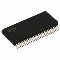
IC CLOCK SYNTHESIZER 56-TSSOP
Manufacturer
Cypress Semiconductor Corp
Type
Clock Synchronizer, Fanout Distribution, Spread Spectrum Clock Generatorr
Datasheet
1.CY28346OXC.pdf
(20 pages)
Specifications of CY28346ZXC
Pll
Yes
Input
Clock, Crystal
Output
Clock
Number Of Circuits
1
Ratio - Input:output
5:17
Differential - Input:output
No/Yes
Frequency - Max
200MHz
Divider/multiplier
Yes/No
Voltage - Supply
3.135 V ~ 3.465 V
Operating Temperature
0°C ~ 70°C
Mounting Type
Surface Mount
Package / Case
56-TSSOP II
Frequency-max
200MHz
Lead Free Status / RoHS Status
Lead free / RoHS Compliant
Available stocks
Company
Part Number
Manufacturer
Quantity
Price
Company:

Part Number:
CY28346ZXC-2
Manufacturer:
CY
Quantity:
63
Part Number:
CY28346ZXC-2
Manufacturer:
CYPRESS/赛普拉斯
Quantity:
20 000
Company:
Part Number:
CY28346ZXC2T
Manufacturer:
CYPR
Quantity:
2 611
Part Number:
CY28346ZXCT
Manufacturer:
CYPRESS/赛普拉斯
Quantity:
20 000


Document #: 38-07331 Rev. *C
Two-Wire SMBus Control Interface
The two-wire control interface implements a Read/Write slave
only interface according to SMBus specification.
The device will accept data written to the D2 address and data
may read back from address D3. It will not respond to any
other addresses, and previously set control registers are
retained as long as power in maintained on the device.
Byte 0: CPU Clock Register
Byte 1: CPU Clock Register
Notes:
2. PU = internal pull-up. PD = internal pull-down. T = tri-level logic input with valid logic voltages of LOW = < 0.8V, T = 1.0 – 1.8V and HIGH = > 2.0V.
3. The “Pin#” column lists the relevant pin number where applicable. The “@Pup” column gives the default state at power-up.
Bit
Bit
7
6
5
4
3
2
1
0
7
6
5
4
3
2
1
0
@Pup
Pin 53
Pin 34
Pin 40
Pin 55
Pin 54
@Pup
Pin 43
0
0
0
0
0
0
0
1
1
1
10,11,12,13,16
44,45,48,49,5
,17,18
Pin#
1,52
35
44,45
48,49
51,52
44,45
48,49
51,52
Pin#
43
53
[2,3]
Spread Spectrum Enable. 0 = Spread Off, 1 = Spread On
This is a Read and Write control bit.
CPU Clock Power-down Mode Select. 0 = Drive CPUT(0:2) to 4 or 6 IREF and drive
CPUC(0:2) LOW when PD# is asserted LOW. 1 = Tri-state all CPU outputs. This is only
applicable when PD# is LOW. It is not applicable to CPU_STP#.
3V66_1/VCH Frequency Select, 0 = 66M selected, 1 = 48M selected
This is a Read and Write control bit.
CPU_STP#. Reflects the current value of the external CPU_STP# (pin 53) This bit is
Read-only.
Reflects the current value of the internal PCI_STP# function when read. Internally PCI_STP#
is a logical AND function of the internal SMBus register bit and the external PCI_STP# pin.
Frequency Select Bit 2. Reflects the value of SEL2 (pin 40). This bit is Read-only.
Frequency Select Bit 1. Reflects the value of SEL1 (pin 55). This bit is Read-only.
Frequency Select Bit 0. Reflects the value of SEL0 (pin 54). This bit is Read-only.
MULT0 (Pin 43) Value. This bit is Read-only.
CPUT/C(0:2) Output Functionality Control When CPU_STP# is Asserted. 0 = Drive
CPUT(0:2) to 4 or 6 IREF and drive CPUC(0:2) LOW when CPU_STP# asserted LOW.
1 = three-state all CPU outputs. This bit will override Byte0,Bit6 such that even if it is 0,
when PD# goes LOW the CPU outputs will be three-stated.
CPU2 Functionality Control When CPU_STP# is Asserted LOW. 1 = Free Running, 0 =
Stopped LOW with CPU_STP# asserted LOW. This is a Read and Write control bit.
CPU1 Functionality Control When CPU_STP# is Asserted LOW. 1 = Free Running, 0 =
Stopped LOW with CPU_STP# asserted LOW. This is a Read and Write control bit.
CPUT0 Functionality Control When CPU_STP# is Asserted LOW. 1 = Free Running, 0 =
Stopped LOW with CPU_STP# asserted LOW. This is a Read and Write control bit.
CPUT/C2 Output Control. 1 = enabled, 0 = disable HIGH and CPUC2 disables LOW. This
is a Read and Write control bit.
CPUT/C1 Output Control. 1 = enabled, 0 = disable HIGH and CPUC1 disables LOW. This
is a Read and Write control bit.
CPUT/C0 Output Control. 1 = enabled, 0 = disable HIGH and CPUC0 disables LOW. This
is a Read and Write control bit.
Serial Control Registers
Following the acknowledge of the Address Byte, two additional
bytes must be sent:
Although the data (bits) in the command is considered “don’t
care,” it must be sent and will be acknowledged. After the
Command Code and the Byte Count have been acknowl-
edged, the sequence (Byte 0, Byte 1, and Byte 2) described
below will be valid and acknowledged.
1. “Command code” byte
2. “Byte count” byte.
Description
Description
CY28346
Page 3 of 20
Related parts for CY28346ZXC
Image
Part Number
Description
Manufacturer
Datasheet
Request
R

Part Number:
Description:
Manufacturer:
Cypress Semiconductor Corp
Datasheet:
Part Number:
Description:
Manufacturer:
Cypress Semiconductor Corp
Datasheet:
Part Number:
Description:
Manufacturer:
Cypress Semiconductor Corp
Datasheet:
Part Number:
Description:
Manufacturer:
Cypress Semiconductor Corp
Datasheet:
Part Number:
Description:
Manufacturer:
Cypress Semiconductor Corp
Datasheet: