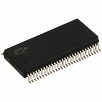
CY28346ZXC Cypress Semiconductor Corp, CY28346ZXC Datasheet - Page 8

CY28346ZXC
Manufacturer Part Number
CY28346ZXC
Description
IC CLOCK SYNTHESIZER 56-TSSOP
Manufacturer
Cypress Semiconductor Corp
Type
Clock Synchronizer, Fanout Distribution, Spread Spectrum Clock Generatorr
Datasheet
1.CY28346OXC.pdf
(20 pages)
Specifications of CY28346ZXC
Pll
Yes
Input
Clock, Crystal
Output
Clock
Number Of Circuits
1
Ratio - Input:output
5:17
Differential - Input:output
No/Yes
Frequency - Max
200MHz
Divider/multiplier
Yes/No
Voltage - Supply
3.135 V ~ 3.465 V
Operating Temperature
0°C ~ 70°C
Mounting Type
Surface Mount
Package / Case
56-TSSOP II
Frequency-max
200MHz
Lead Free Status / RoHS Status
Lead free / RoHS Compliant
Available stocks
Company
Part Number
Manufacturer
Quantity
Price
Company:
Part Number:
CY28346ZXC-2
Manufacturer:
CY
Quantity:
63
Part Number:
CY28346ZXC-2
Manufacturer:
CYPRESS/赛普拉斯
Quantity:
20 000
Company:
Part Number:
CY28346ZXC2T
Manufacturer:
CYPR
Quantity:
2 611
Part Number:
CY28346ZXCT
Manufacturer:
CYPRESS/赛普拉斯
Quantity:
20 000
Document #: 38-07331 Rev. *C
Table 4. Host Clock (HCSL) Buffer Characteristics
Table 5. CPU Clock Current Select Function
Table 6. Group Timing Relationship and Tolerances
USB and DOT 48M Phase Relationship
The 48MUSB and 48MDOT clocks are in phase. It is under-
stood that the difference in edge rate will introduce some
inherent offset. When 3V66_1/VCH clock is configured for
VCH (48-MHz) operation it is also in phase with the USB and
DOT outputs. See Figure 5.
66IN to 66B(0:2) Buffered Prop Delay
The 66IN to 66B(0:2) output delay is shown in Figure 6.
The Tpd is the prop delay from the input pin (66IN) to the
output pins (66B[0:2]). The outputs’ variation of Tpd is
described in the AC parameters section of this data sheet. The
measurement taken at 1.5V.
3V66 to PCI
48MUSB to 48MDOT Skew
66B(0:2) to PCI offset
Mult0
PCIF(0:2)
66B(0:2)
0
1
PCI(0:6)
66B(0:2)
66IN
48MUSB
48MDOT
Description
Board Target Trace/Term Z
Vout
Ros
Ro
Tpd
3.5ns
1.5-
Figure 7. Buffer Mode – 33V66(0:1); 66BUF(0:2) Phase Relationship
50Ω
50Ω
Figure 5. 48MUSB and 48MDOT Phase Relationship
Figure 6. 66IN to 66B(0:2) Output Delay Figure
Offset
2.5 ns
0.0 ns
2.5 ns
3000Ω (recommended)
Reference R, Iref – Vdd (3*Rr)
Rr = 221 1%, Iref = 5.00mA
Rr = 475 1%, Iref = 2.32mA
N/A
Tolerance
66B(0:2) to PCI Buffered Clock Skew
Figure 7 shows the difference (skew) between the 3V33(0:5)
outputs when the 66M clocks are connected to 66IN. This
offset is described in the Group Timing Relationship and Toler-
ances section of this data sheet. The measurements were
taken at 1.5V.
3V66 to PCI Un-Buffered Clock Skew
Figure 8 shows the timing relationship between 3V66(0:5) and
PCI(0:6) and PCI_F(0:2) when configured to run in the unbuf-
fered mode.
±1.0 ns
±1.0 ns
±1.0 ns
3V66 Leads PCI (unbuffered mode)
0 degrees phase shift
66B Leads PCI (buffered mode)
Output Current
Ioh = 4*Iref
Ioh = 6*Iref
Conditions
1.2V
N/A
CY28346
1.0V @ 50
0.7V @ 50
Page 8 of 20
Voh @ Z


