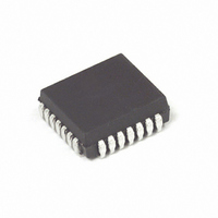
MC88915FN70R2 Freescale Semiconductor, MC88915FN70R2 Datasheet - Page 3

MC88915FN70R2
Manufacturer Part Number
MC88915FN70R2
Description
IC DRIVER CLK PLL 70MHZ 28-PLCC
Manufacturer
Freescale Semiconductor
Type
Clock Driver, Fanout Distribution, Multiplexerr
Datasheet
1.MC88915FN55.pdf
(13 pages)
Specifications of MC88915FN70R2
Pll
Yes
Input
TTL
Output
CMOS, TTL
Number Of Circuits
1
Ratio - Input:output
3:8
Differential - Input:output
No/No
Frequency - Max
70MHz
Divider/multiplier
Yes/Yes
Voltage - Supply
4.75 V ~ 5.25 V
Operating Temperature
0°C ~ 70°C
Mounting Type
Surface Mount
Package / Case
28-PLCC
Frequency-max
70MHz
Lead Free Status / RoHS Status
Contains lead / RoHS non-compliant
Other names
MC88915FN70R2TR
Available stocks
Company
Part Number
Manufacturer
Quantity
Price
Company:
Part Number:
MC88915FN70R2
Manufacturer:
MOTOROLA
Quantity:
268
Company:
Part Number:
MC88915FN70R2
Manufacturer:
Freescale Semiconductor
Quantity:
10 000
Part Number:
MC88915FN70R2
Manufacturer:
MOTOROLA/摩托罗拉
Quantity:
20 000
DC ELECTRICAL CHARACTERISTICS (Voltages Referenced to GND; T A =0 C to + 70 C, V CC = 5.0V
1. I OL and I OH are 12mA and –12mA respectively for the LOCK output.
2. The PLL_EN input pin is not guaranteed to meet this specification.
3. Maximum test duration is 2.0ms, one output loaded at a time.
CAPACITANCE AND POWER SPECIFICATIONS
SYNC INPUT TIMING REQUIREMENTS
1. Information in Fig. 5 and in the “General AC Specification Notes”, Note #3 describes this specification and its actual limits depending on the
FREQUENCY SPECIFICATIONS (T A =0 C to + 70 C, V CC = 5.0V 5%, C L = 50pF)
1. Maximum Operating Frequency is guaranteed with the part in a phase–locked condition, and all outputs loaded at 50 pF.
TIMING SOLUTIONS
BR1333 — Rev 6
Symbol
I OHD
I CCT
I OLD
V OH
V OL
application.
V IH
I CC
t RISE , t FALL
V IL
I in
Duty Cycle
Symbol
Symbol
t CYCLE
t CYCLE
Symbol
f max 1
C PD
PD 1
PD 2
C IN
Minimum High–Level Input
Voltage
Maximum Low–Level Input
Voltage
Minimum High–Level Output
Voltage
Maximum Low–Level Output
Voltage
Maximum Input Leakage Current
Maximum I CC /Input
Minimum Dynamic Output Current 3
Maximum Quiescent Supply
Current (per Package)
Input Capacitance
Power Dissipation Capacitance
Power Dissipation @ 33MHz with 50 Thevenin Termination
Power Dissipation @ 33MHz with 50 Parallel Termination to GND
Maximum Rise and Fall times, (SYNC Inputs: From 0.8V – 2.0V)
Input Clock Period (SYNC Inputs)
Input Clock Period (SYNC Inputs)
Input Duty Cycle (SYNC Inputs)
Maximum Operating Frequency (2X_Q Output)
Maximum Operating Frequency (Q0–Q4,Q5 Output)
Parameter
Parameter
Parameter
Parameter
V out = 0.1 V or V CC – 0.1 V
V out = 0.1 V or V CC – 0.1 V
V in = V IH or V IL
V in = V IH or V IL
V I = V CC or GND
V I = V CC – 2.1 V
V OLD = 1.0V Max
V OHD = 3.85 V Max
V I = V CC or GND
I OH = –36 mA 1
I OL = 36 mA 1
3
Test Conditions
37.5 mW/Output
120 mW/Device
300 mW/Device
MC88915FN55
FN55
Typical Values
15 mW/Output
36
Guaranteed Minimum
27.5
V CC
Min
4.75
5.25
4.75
5.25
4.75
5.25
4.75
5.25
5.25
5.25
5.25
5.25
5.25
4.5
55
40
–
V
FN70
28.5
50% 25%
Guaranteed Limit
MC88915FN70
Unit
mW
mW
pF
pF
1.5 2
4.01
4.51
0.44
0.44
–88
2.0
2.0
0.8
0.8
1.0
88
1.0
5%)
200 1
200 1
Max
3.0
70
35
MC88915
V CC = 5.0 V
V CC = 5.0 V
V CC = 5.0 V
V CC = 5.0 V
Conditions
T = 25 C
T = 25 C
MOTOROLA
MHz
MHz
Unit
Unit
Unit
ns
ns
ns
mA
mA
mA
mA
V
V
V
V
A


