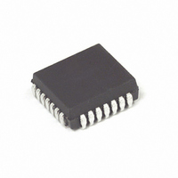
MC88915FN70R2 Freescale Semiconductor, MC88915FN70R2 Datasheet - Page 6

MC88915FN70R2
Manufacturer Part Number
MC88915FN70R2
Description
IC DRIVER CLK PLL 70MHZ 28-PLCC
Manufacturer
Freescale Semiconductor
Type
Clock Driver, Fanout Distribution, Multiplexerr
Datasheet
1.MC88915FN55.pdf
(13 pages)
Specifications of MC88915FN70R2
Pll
Yes
Input
TTL
Output
CMOS, TTL
Number Of Circuits
1
Ratio - Input:output
3:8
Differential - Input:output
No/No
Frequency - Max
70MHz
Divider/multiplier
Yes/Yes
Voltage - Supply
4.75 V ~ 5.25 V
Operating Temperature
0°C ~ 70°C
Mounting Type
Surface Mount
Package / Case
28-PLCC
Frequency-max
70MHz
Lead Free Status / RoHS Status
Contains lead / RoHS non-compliant
Other names
MC88915FN70R2TR
Available stocks
Company
Part Number
Manufacturer
Quantity
Price
Company:
Part Number:
MC88915FN70R2
Manufacturer:
MOTOROLA
Quantity:
268
Company:
Part Number:
MC88915FN70R2
Manufacturer:
Freescale Semiconductor
Quantity:
10 000
Part Number:
MC88915FN70R2
Manufacturer:
MOTOROLA/摩托罗拉
Quantity:
20 000
MC88915
EXTERNAL LOOP FILTER
MOTOROLA
5. The t SKEWr specification guarantees that the rising edges
With the 470K resistor tied in this fashion, the t PD specification
measured at the input pins is:
of outputs Q/2, Q0, Q1, Q2, Q3, and Q4 will always fall
within a 500ps window within one part. However, if the
relative position of each output within this window is not
specified, the 500 ps window must be added to each side
of the tPD specification limits to calculate the total
part–to–part skew. For this reason the absolute
FEEDBACK OUTPUT
SYNC INPUT
Table 2. Relative Positions of Outputs Q/2, Q0–Q4, 2X_Q, Within the 500ps t SKEWr Spec Window
t PD = 2.25ns 1.0ns
0.1 F
Figure 2. Depiction of the Fixed SYNC to Feedback Offset (tPD) Which is
330
RC1
Present When a 470K Resistor is Tied to VCC or Ground
2.25ns OFFSET
R2
C1
ANALOG GND
Output
2X_Q
Q/2
Q0
Q1
Q2
Q3
Q4
REFERENCE
3.0V
RESISTOR
470K
5.0V
–274
–633
(ps)
–72
–44
–40
–16
6
–
0
distribution of these outputs are provided in table 2. When
taking the skew data, Q0 was used as a reference, so all
measurements are relative to this output. The information
in Table 2 is derived from measurements taken from the
14 process lots described in Note 1, over the temperature
and voltage range.
With the 470K resistor tied in this fashion, the t PD specification
measured at the input pins is:
FEEDBACK OUTPUT
REFERENCE
RESISTOR
SYNC INPUT
(ps)
276
255
–34
250
–35
40
470K
+
0
ANALOG VCC
t PD = –0.775ns 0.275ns
0.1 F
330
C1
RC1
R2
ANALOG GND
–0.775ns OFFSET
TIMING SOLUTIONS
BR1333 — Rev 6
5.0V
3.0V


