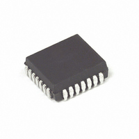
MC88915FN70R2 Freescale Semiconductor, MC88915FN70R2 Datasheet - Page 8

MC88915FN70R2
Manufacturer Part Number
MC88915FN70R2
Description
IC DRIVER CLK PLL 70MHZ 28-PLCC
Manufacturer
Freescale Semiconductor
Type
Clock Driver, Fanout Distribution, Multiplexerr
Datasheet
1.MC88915FN55.pdf
(13 pages)
Specifications of MC88915FN70R2
Pll
Yes
Input
TTL
Output
CMOS, TTL
Number Of Circuits
1
Ratio - Input:output
3:8
Differential - Input:output
No/No
Frequency - Max
70MHz
Divider/multiplier
Yes/Yes
Voltage - Supply
4.75 V ~ 5.25 V
Operating Temperature
0°C ~ 70°C
Mounting Type
Surface Mount
Package / Case
28-PLCC
Frequency-max
70MHz
Lead Free Status / RoHS Status
Contains lead / RoHS non-compliant
Other names
MC88915FN70R2TR
Available stocks
Company
Part Number
Manufacturer
Quantity
Price
Company:
Part Number:
MC88915FN70R2
Manufacturer:
MOTOROLA
Quantity:
268
Company:
Part Number:
MC88915FN70R2
Manufacturer:
Freescale Semiconductor
Quantity:
10 000
Part Number:
MC88915FN70R2
Manufacturer:
MOTOROLA/摩托罗拉
Quantity:
20 000
MC88915
MOTOROLA
SYNC INPUT
(SYNC[1] or
FEEDBACK
Q/2 OUTPUT
SYNC[0])
2X_Q OUTPUT
Q5 OUTPUT
Q0 – Q4
OUTPUTS
INPUT
t SKEWALL
Timing Notes:
The MC88915 aligns rising edges of the FEEDBACK input and SYNC input, therefore the SYNC input does
All skew specs are measured between the V CC /2 crossing point of the appropriate output edges.All skews
If a “Q” output is connected to the FEEDBACK input (this situation is not shown), the “Q” output frequency
not require a 50% duty cycle.
are specified as ‘windows’, not as a
would match the SYNC input frequency, the 2X_Q output would run at twice the SYNC frequency, and the
Q/2 output would run at half the SYNC frequency.
(These waveforms represent the hook–up configuration of Figure 5a on page 9)
Figure 4. Output / Input Switching Waveforms and Timing Diagrams
t
PD
t SKEWf
deviation around a center point.
t CYCLE SYNC INPUT
8
t SKEWr
t CYCLE “Q” OUTPUTS
t SKEWf
TIMING SOLUTIONS
BR1333 — Rev 6
t SKEWR


