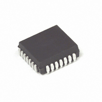
MC88915FN70R2 Freescale Semiconductor, MC88915FN70R2 Datasheet - Page 9

MC88915FN70R2
Manufacturer Part Number
MC88915FN70R2
Description
IC DRIVER CLK PLL 70MHZ 28-PLCC
Manufacturer
Freescale Semiconductor
Type
Clock Driver, Fanout Distribution, Multiplexerr
Datasheet
1.MC88915FN55.pdf
(13 pages)
Specifications of MC88915FN70R2
Pll
Yes
Input
TTL
Output
CMOS, TTL
Number Of Circuits
1
Ratio - Input:output
3:8
Differential - Input:output
No/No
Frequency - Max
70MHz
Divider/multiplier
Yes/Yes
Voltage - Supply
4.75 V ~ 5.25 V
Operating Temperature
0°C ~ 70°C
Mounting Type
Surface Mount
Package / Case
28-PLCC
Frequency-max
70MHz
Lead Free Status / RoHS Status
Contains lead / RoHS non-compliant
Other names
MC88915FN70R2TR
Available stocks
Company
Part Number
Manufacturer
Quantity
Price
Company:
Part Number:
MC88915FN70R2
Manufacturer:
MOTOROLA
Quantity:
268
Company:
Part Number:
MC88915FN70R2
Manufacturer:
Freescale Semiconductor
Quantity:
10 000
Part Number:
MC88915FN70R2
Manufacturer:
MOTOROLA/摩托罗拉
Quantity:
20 000
TIMING SOLUTIONS
BR1333 — Rev 6
CRYSTAL
OSCILLATOR
CRYSTAL
OSCILLATOR
CRYSTAL
OSCILLATOR
12.5 MHz INPUT
25 MHZ INPUT
50 MHz INPUT
Figure 5a. Wiring Diagram and Frequency Relationships With Q/2 Output Feed Back
Figure 5b. Wiring Diagram and Frequency Relationships With Q4 Output Feed Back
Figure 5c. Wiring Diagram and Frequency Relationships with 2X_Q Output Feed Back
EXTERNAL
LOOP
FILTER
EXTERNAL
LOOP
FILTER
EXTERNAL
LOOP
FILTER
LOW
LOW
LOW
25 MHz FEEDBACK SIGNAL
SYNC[0]
FQ_SEL
SYNC[0]
FQ_SEL
SYNC[0]
FQ_SEL
FEEDBACK
REF_SEL
ANALOG V CC
RC1
ANALOG GND
FEEDBACK
REF_SEL
ANALOG V CC
RC1
ANALOG GND
FEEDBACK
REF_SEL
ANALOG V CC
RC1
ANALOG GND
HIGH
HIGH
12.5 MHz FEEDBACK SIGNAL
HIGH
RST
HIGH
RST
RST
HIGH
HIGH
50 MHz FEEDBACK SIGNAL
Q0
Q5
Q0
Q0
Q5
Q5
MC88915
MC88915
MC88915
Q4
Q1
Q1
Q1
Q4
Q4
PLL_EN
PLL_EN
PLL_EN
2X_Q
2X_Q
2X_Q
Q/2
HIGH
Q/2
Q/2
HIGH
Q3
Q2
HIGH
Q3
Q2
Q3
Q2
50 MHz SIGNAL
50 MHz SIGNAL
12.5 MHz
SIGNAL
12.5 MHz
SIGNAL
9
OUTPUTS
OUTPUTS
OUTPUTS
5MHz to (2X_Q FMAX Spec)/4 (for FREQ_SEL HIGH)
2.5MHz to (2X_Q FMAX Spec)/8 (for FREQ_SEL LOW)
CLOCK
CLOCK
CLOCK
25MHz
25MHz
25MHz
10MHz to (2X_Q FMAX Spec)/2 (for FREQ_SEL HIGH)
5MHz to (2X_Q FMAX Spec)/4 (for FREQ_SEL LOW)
20MHz to (2X_Q FMAX Spec) (for FREQ_SEL HIGH)
10MHz to (2X_Q FMAX Spec)/2 (for FREQ_SEL LOW)
“Q”
“Q”
“Q”
Allowable Input Frequency Range:
1:2 Input to “Q” Output Frequency Relationship
1:1 Input to “Q” Output Frequency Relationship
2:1 Input to “Q” Output Frequency Relationship
Allowable Input Frequency Range:
Allowable Input Frequency Range:
In this application, the Q4 output is connected to
the FEEDBACK input. The internal PLL will line up
the positive edges of Q4 and SYNC, thus the Q4
frequency (and the rest of the “Q” outputs) will
equal the SYNC frequency. The Q/2 output will al-
ways run at 1/2 the “Q” frequency, and the 2X_Q
output will run at 2X the “Q” frequency.
In this application, the Q/2 output is connected to
the FEEDBACK input. The internal PLL will line up
the positive edges of Q/2 and SYNC, thus the Q/2
frequency will equal the SYNC frequency. The “Q”
outputs (Q0–Q4, Q5) will always run at 2X the Q/2
frequency, and the 2X_Q output will run at 4X the
Q/2 frequency.
In this application, the 2X_Q output is connected
to the FEEDBACK input. The internal PLL will line
up the positive edges of 2X_Q and SYNC, thus the
2X_Q frequency will equal the SYNC frequency.
The Q/2 output will always run at 1/4 the 2X_Q fre-
quency, and the “Q” outputs will run at 1/2 the
2X_Q frequency.
MC88915
MOTOROLA


