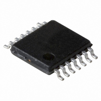
PCF2123TS/1,118 NXP Semiconductors, PCF2123TS/1,118 Datasheet - Page 41

PCF2123TS/1,118
Manufacturer Part Number
PCF2123TS/1,118
Description
IC SPI RTC/CALENDAR 14TSSOP
Manufacturer
NXP Semiconductors
Type
Clock/Calendar/Alarmr
Specifications of PCF2123TS/1,118
Package / Case
14-TSSOP
Time Format
HH:MM:SS (12/24 hr)
Date Format
YY-MM-DD-dd
Interface
SPI, 3-Wire Serial
Voltage - Supply
1.1 V ~ 5.5 V
Operating Temperature
-40°C ~ 85°C
Mounting Type
Surface Mount
Function
Clock/Calendar
Supply Voltage (max)
5.5 V
Supply Voltage (min)
1.1 V
Maximum Operating Temperature
+ 85 C
Minimum Operating Temperature
- 40 C
Mounting Style
SMD/SMT
Rtc Bus Interface
Serial (3-Wire, SPI)
Lead Free Status / RoHS Status
Lead free / RoHS Compliant
Memory Size
-
Lead Free Status / Rohs Status
Lead free / RoHS Compliant
Other names
568-4534-2
935286384118
PCF2123TS/1-T
935286384118
PCF2123TS/1-T
Available stocks
Company
Part Number
Manufacturer
Quantity
Price
Company:
Part Number:
PCF2123TS/1,118
Manufacturer:
VISHAY
Quantity:
15 160
Part Number:
PCF2123TS/1,118
Manufacturer:
NXP/恩智浦
Quantity:
20 000
NXP Semiconductors
Table 44.
V
specified.
[1]
[2]
[3]
[4]
[5]
[6]
PCF2123
Product data sheet
Symbol
Inputs
V
V
V
I
R
C
Outputs
V
V
V
I
I
I
C
R
LI
OH
OL
LO
DD
IL
IH
I
O
OH
OL
pd
i
L(itg)
s
= 1.1 V to 5.5 V; V
For reliable oscillator start at power-on: V
Timer source clock =
In case of an ESD event, the value may increase slightly.
Implicit by design.
Refers to external pull-up voltage.
Integrated load capacitance, C
Static characteristics
Parameter
LOW-level input voltage
HIGH-level input voltage
input voltage
input leakage current
pull-down resistance
input capacitance
output voltage
HIGH-level output voltage on pin SDO
LOW-level output voltage
HIGH-level output current
LOW-level output current
output leakage current
integrated load
capacitance
series resistance
SS
1
⁄
60
= 0 V; T
Hz, level of pins CE, SDI, and SCL is V
L(itg)
amb
, is a calculation of C
…continued
=
−
40
DD
All information provided in this document is subject to legal disclaimers.
Conditions
on pins CE, SDI, SCL, OSCI,
CLKOE, CLKOUT
V
SCL, OSCI, CLKOE, CLKOUT
V
on pin CE
on pins SDI, SCL, CLKOE and
CE
on pins CLKOUT and INT
on pin OSCO
on pin SDO
on pin SDO
on pins CLKOUT and INT;
V
I
output source current;
V
V
output sink current;
V
V
and CLKOUT
V
on pins OSCO and OSCI
OL
= V
°
I
I
DD
OH
DD
OL
DD
O
C to +85
= V
= V
= 1.5 mA
= V
DD(min)
= 0.4 V;
= 5 V;
= 5 V on pin SDO
= 5 V on pins INT, SDO
= 4.6 V;
DD
SS
DD
Rev. 5 — 27 April 2011
on pin CE
or V
+ 0.3 V.
or V
OSCI
°
C; f
SS
SS
and C
osc
on pins SDI,
= 32.768 kHz; quartz R
DD
OSCO
or V
SS
in series:
.
[3]
[4]
[5]
[3]
[6]
C
L itg
Min
-
0.7V
−0.5
-
−1
-
-
−0.5
−0.5
−0.5
0.8V
V
V
1.5
1.5
-
3.3
-
(
SS
SS
)
DD
DD
=
s
= 15 k
------------------------------------------- -
(
(
C
C
OSCI
OSCI
SPI Real time clock/calendar
Typ
-
-
-
0
0
240
-
-
-
-
-
-
-
-
-
0
7
-
Ω
; C
+
⋅
C
C
L
OSCO
OSCO
= 7 pF; unless otherwise
)
)
PCF2123
© NXP B.V. 2011. All rights reserved.
Max
0.3V
-
+5.5
-
-
550
7
+5.5
+5.5
V
V
0.2V
0.4
-
-
-
14
100
.
DD
DD
DD
+ 0.5
DD
Unit
V
V
V
μA
μA
kΩ
pF
V
V
V
V
V
V
mA
mA
μA
pF
kΩ
41 of 63


