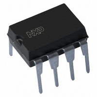
PCF8593P,112 NXP Semiconductors, PCF8593P,112 Datasheet - Page 9

PCF8593P,112
Manufacturer Part Number
PCF8593P,112
Description
IC CLOCK/CALENDAR LOW PWR 8-DIP
Manufacturer
NXP Semiconductors
Type
Clock/Calendar/NVSRAMr
Datasheet
1.PCF8593T1118.pdf
(35 pages)
Specifications of PCF8593P,112
Package / Case
8-DIP (0.300", 7.62mm)
Time Format
HH:MM:SS:hh (12/24 hr)
Date Format
YY-MM-DD-dd
Memory Size
8B
Interface
I²C, 2-Wire Serial
Voltage - Supply
1 V ~ 6 V
Operating Temperature
-40°C ~ 85°C
Mounting Type
Through Hole
Function
Clock/Calendar/Alarm/Timer Interrupt
Rtc Memory Size
8 Byte
Supply Voltage (max)
6 V
Supply Voltage (min)
1 V
Maximum Operating Temperature
+ 85 C
Minimum Operating Temperature
- 40 C
Mounting Style
Through Hole
Rtc Bus Interface
Serial (I2C)
Bus Type
Serial (I2C)
User Ram
8Byte
Package Type
PDIP
Operating Supply Voltage (max)
6V
Operating Temperature Classification
Industrial
Operating Temperature (max)
85C
Operating Temperature (min)
-40C
Pin Count
8
Mounting
Through Hole
Lead Free Status / RoHS Status
Lead free / RoHS Compliant
Lead Free Status / RoHS Status
Lead free / RoHS Compliant, Lead free / RoHS Compliant
Other names
568-1089-5
935151750112
PCF8593N
935151750112
PCF8593N
NXP Semiconductors
PCF8593
Product data sheet
7.6 Alarm registers
All alarm registers are allocated with a constant address offset of 08h to the
corresponding counter registers (see
An alarm signal is generated when the contents of the alarm registers match bit-by-bit the
contents of the involved counter registers. The year and weekday bits are ignored in a
dated alarm. A daily alarm ignores the month and date bits. When a weekday alarm is
selected, the contents of the alarm weekday and month register selects the weekdays on
which an alarm is activated (see
Remark: In the 12 hour mode, bits 6 and 7 of the alarm hours register must be the same
as the hours counter.
Fig 9.
Alarm control registers, clock mode
MSB
7
013aaa387
All information provided in this document is subject to legal disclaimers.
6
Rev. 04 — 6 October 2010
5
4
3
Figure
2
Figure
10).
1
8).
LSB
0
alarm interrupt enable:
(only valid when alarm enable in
the control and status register is set)
0
1
clock alarm function:
memory location 08h
timer function:
000
001
010
011
100
101
110
111
timer interrupt enable:
00
01
10
11
timer alarm enable:
0
1
0
1
Low power clock and calendar
no timer alarm
timer alarm
no timer
hundredths of a second
seconds
minutes
hours
days
not used
test mode, all counters
in parallel
alarm flag, no interrupt
alarm flag, interrupt
timer flag, no interrupt
timer flag, interrupt
no clock alarm
daily alarm
weekday alarm
dated alarm
PCF8593
© NXP B.V. 2010. All rights reserved.
9 of 35


