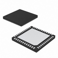
MAX5865ETM+ Maxim Integrated Products, MAX5865ETM+ Datasheet - Page 19

MAX5865ETM+
Manufacturer Part Number
MAX5865ETM+
Description
IC ANLG FRONT END 40MSPS 48-TQFN
Manufacturer
Maxim Integrated Products
Datasheet
1.MAX5865ETM.pdf
(26 pages)
Specifications of MAX5865ETM+
Number Of Bits
10
Number Of Channels
4
Power (watts)
2.10W
Voltage - Supply, Analog
2.7 V ~ 3.3 V
Voltage - Supply, Digital
1.8 V ~ 3.3 V
Package / Case
48-TQFN Exposed Pad
Lead Free Status / RoHS Status
Lead free / RoHS Compliant
Clock jitter is especially critical for undersampling
applications. Consider the clock input as an analog
input and route away from any analog input or other
digital signal lines. The MAX5865 clock input operates
with an OV
±15% duty cycle.
The MAX5865 features an internal precision 1.024V
bandgap reference that is stable over the entire power
supply and temperature range. The REFIN input pro-
vides two modes of reference operation. The voltage at
REFIN (V
In internal reference mode, connect REFIN to V
V
and REFN are low-impedance outputs with V
V
V
0.33µF capacitor. Bypass REFIN to GND with a 0.1µF
capacitor.
In buffered external reference mode, apply 1.024V
±10% at REFIN. In this mode, COM, REFP, and REFN
are low-impedance outputs with V
= V
Bypass REFP, REFN, and COM each with a 0.33µF
capacitor. Bypass REFIN to GND with a 0.1µF capaci-
tor. In this mode, the DAC’s full-scale output voltage
and common-mode voltage are proportional to the
external reference. For example, if the V
increased by 10% (max), the DACs’ full-scale output
voltage is also increased by 10% or to ±440mV, and
the common-mode voltage increases by 10%.
Table 4. Reference Modes
REF
DD
REF
1.024V ±10%
>0. 8 x V
DD
/2, V
/2. Bypass REFP, REFN, and COM each with a
V
is an internally generated 0.512V. COM, REFP,
REFIN
/2 + V
REFIN
REFP
DD
DD
REFIN
/2 voltage threshold and accepts a 50%
) sets reference operation mode
= V
DD
Internal reference mode. V
generated to be 0.512V. Bypass REFP,
REFN, and COM each with a 0.33µF
capacitor.
Buffered external reference mode. An
external 1.024V ±10% reference voltage
is applied to REFIN. V
generated to be V
REFN, and COM each with a 0.33µF
capacitor. Bypass REFIN to GND with a
0.1µF capacitor.
______________________________________________________________________________________
/4, and V
Performance, 40Msps Analog Front End
/2 + V
Reference Configurations
REF
REFERENCE MODE
REFN
/2, and V
REFIN
COM
= V
REF
Ultra-Low-Power, High-Dynamic-
/2. Bypass REFP,
DD
= V
REFN
is internally
REF
/2 - V
DD
is internally
= V
(Table
/2, V
REFIN
REFIN
COM
DD
REFP
DD
/2 -
4).
/4.
is
=
.
An RF transformer
solution to convert a single-ended signal source to a
fully differential signal for optimum ADC performance.
Connecting the center tap of the transformer to COM
provides a V
former can be used, or a step-up transformer can be
selected to reduce the drive requirements. In general,
the MAX5865 provides better SFDR and THD with fully
differential input signals than single-ended signals,
especially for high-input frequencies. In differential
mode, even-order harmonics are lower as both inputs
(IA+, IA-, QA+, QA-) are balanced, and each of the
ADC inputs only requires half the signal swing com-
pared to single-ended mode.
transformer converting the MAX5865 DACs’ differential
analog outputs to single ended.
Figure 7. Balun-Transformer Coupled Single-Ended to
Differential Input Drive for ADCs
V
V
IN
IN
Using Balun Transformer AC-Coupling
0.1µF
0.1µF
DD
/2 DC level shift to the input. A 1:1 trans-
Applications Information
0.33µF
0.33µF
(Figure
25Ω
25Ω
25Ω
25Ω
0.1µF
0.1µF
7) provides an excellent
22pF
22pF
22pF
22pF
Figure 8
IA+
COM
IA-
QA+
QA-
shows an RF
MAX5865
19


