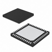
MAX5865ETM+ Maxim Integrated Products, MAX5865ETM+ Datasheet - Page 20

MAX5865ETM+
Manufacturer Part Number
MAX5865ETM+
Description
IC ANLG FRONT END 40MSPS 48-TQFN
Manufacturer
Maxim Integrated Products
Datasheet
1.MAX5865ETM.pdf
(26 pages)
Specifications of MAX5865ETM+
Number Of Bits
10
Number Of Channels
4
Power (watts)
2.10W
Voltage - Supply, Analog
2.7 V ~ 3.3 V
Voltage - Supply, Digital
1.8 V ~ 3.3 V
Package / Case
48-TQFN Exposed Pad
Lead Free Status / RoHS Status
Lead free / RoHS Compliant
Ultra-Low-Power, High-Dynamic-
Performance, 40Msps Analog Front End
Figure 8. Balun-Transformer Coupled Differential to Single-
Ended Output Drive for DACs
Figure 9. Single-Ended Drive for ADCs
20
V
V
IN
IN
______________________________________________________________________________________
100Ω
100Ω
100Ω
100Ω
MAX5865
0.1µF
0.1µF
QD+
QD-
ID+
ID-
REFP
REFN
REFP
REFN
1kΩ
1kΩ
1kΩ
1kΩ
R
50Ω
R
50Ω
0.1µF
0.1µF
ISO
ISO
22pF
22pF
22pF
22pF
50Ω
R
C
50Ω
C
C
R
C
ISO
IN
ISO
IN
IN
IN
V
V
OUT
OUT
INA+
COM
INA-
INB+
INB-
MAX5865
Drive the MAX5865 ADCs with op amps when a balun
transformer is not available.
ADCs being driven by op amps for AC-coupled single-
ended, and DC-coupled differential applications.
Amplifiers such as the MAX4354/MAX4454 provide
high speed, high bandwidth, low noise, and low distor-
tion to maintain the input signal integrity.
also be used to interface with the DAC differential ana-
log outputs to provide gain or buffering. The DAC dif-
ferential analog outputs cannot be used in single-
ended mode because of the internally generated
1.4VDC common-mode level. Also, the DAC analog
outputs are designed to drive a differential input stage
with input impedance ≥70kΩ. If single-ended outputs
are desired, use an amplifier to provide differential to
single-ended conversion and select an amplifier with
proper input common-mode voltage range.
The MAX5865 can be used in diverse applications
operating FDD or TDD modes. The MAX5865 operates
in Xcvr mode for FDD applications such as WCDMA-
3GPP (FDD) and 4G technologies. Also, the MAX5865
can switch between Tx and Rx modes for TDD applica-
tions like TD-SCDMA, WCDMA-3GPP (TDD),
IEEE802.11a/b/g, and IEEE802.16.
In FDD mode, the ADC and DAC operate simultaneously.
The ADC bus and DAC bus are dedicated and must be
connected in 18-bit parallel (8-bit ADC and 10-bit DAC)
to the digital baseband processor. Select Xcvr mode
through the 3-wire serial interface and use the conversion
clock to latch data. In FDD mode, the MAX5865 uses
75.6mW power at f
of the ADC and DAC operating simultaneously.
In TDD mode, the ADC and DAC operate independent-
ly. The ADC and DAC bus are shared and can be con-
nected together, forming a single 10-bit parallel bus to
the digital baseband processor. Using the 3-wire serial
interface, select between Rx mode to enable the ADC
and Tx mode to enable the DAC. When operating in Rx
mode, the DAC does not transmit because the core is
disabled and in Tx mode, the ADC bus is tri-state. This
eliminates any unwanted spurious emissions and pre-
vents bus contention. In TDD mode, the MAX5865 uses
63mW power in Rx mode at f
DAC uses 38.4mW in Tx mode.
Figure
MAX2820 in TDD mode to provide a complete 802.11b
radio front-end solution. Because the MAX5865 DAC has
full differential analog outputs with a common-mode level
of 1.4V, and the ADC has wide-input common-mode
11 illustrates the MAX5865 working with the
CLK
= 40MHz. This is the total power
Using Op-Amp Coupling
Figures 9 and 10
FDD and TDD Modes
CLK
= 40MHz, and the
Figure 10
show the
can


