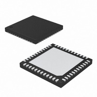
MAX5865ETM+ Maxim Integrated Products, MAX5865ETM+ Datasheet - Page 2

MAX5865ETM+
Manufacturer Part Number
MAX5865ETM+
Description
IC ANLG FRONT END 40MSPS 48-TQFN
Manufacturer
Maxim Integrated Products
Datasheet
1.MAX5865ETM.pdf
(26 pages)
Specifications of MAX5865ETM+
Number Of Bits
10
Number Of Channels
4
Power (watts)
2.10W
Voltage - Supply, Analog
2.7 V ~ 3.3 V
Voltage - Supply, Digital
1.8 V ~ 3.3 V
Package / Case
48-TQFN Exposed Pad
Lead Free Status / RoHS Status
Lead free / RoHS Compliant
ABSOLUTE MAXIMUM RATINGS
V
GND to OGND.......................................................-0.3V to +0.3V
IA+, IA-, QA+, QA-, ID+, ID-, QD+, QD-, REFP, REFN,
DD0–DD9, SCLK, DIN, CS, CLK,
Ultra-Low-Power, High-Dynamic-
Performance, 40Msps Analog Front End
Stresses beyond those listed under “Absolute Maximum Ratings” may cause permanent damage to the device. These are stress ratings only, and functional
operation of the device at these or any other conditions beyond those indicated in the operational sections of the specifications is not implied. Exposure to
absolute maximum rating conditions for extended periods may affect device reliability.
ELECTRICAL CHARACTERISTICS
(V
DAC output amplitude = 0dBFS, differential ADC input, differential DAC output, C
otherwise noted. Typical values are at T
2
POWER REQUIREMENTS
Analog Supply Voltage
Output Supply Voltage
V
OV
DD
DD
REFIN, COM to GND ..............................-0.3V to (V
DA0–DA7 to OGND .............................-0.3V to (OV
DD
DD
_______________________________________________________________________________________
to GND, OV
= 3V, OV
Supply Current
Supply Current
PARAMETER
DD
DD
= 1.8V, internal reference (1.024V), C
to OGND................................-0.3V to +3.3V
SYMBOL
A
OV
= +25°C, unless otherwise noted.) (Note 1)
V
DD
DD
AD C op er ati ng m od e, f
40M H z, D AC op er ati ng m od e, f
ADC operating mode (Rx), f
f
OV
DAC operating mode (Tx), f
f
Standby mode, DAC digital inputs and CLK
at zero or OV
Idle mode, DAC digital inputs at zero or
OV
Shutdown mode, digital inputs and CLK at
zero or OV
ADC operating mode, f
40Msps, DAC operating mode, f
2.2MHz
Idle mode, DAC digital inputs at zero or
OV
Shutdown mode, DAC digital inputs and
CLK at zero or OV
CLK
CLK
DD
DD
D D
DD
DD,
L
= 40M H z, DAC digital inputs at zero or
= 40M H z, ADC off
+ 0.3V)
+ 0.3V)
, f
≈ 10pF on all digital outputs, f
f
CLK
CLK
DD
= 40M H z
= 40M H z
DD
, CS = OV
CONDITIONS
DD
Continuous Power Dissipation (T
Thermal Resistance θ
Operating Temperature Range ...........................-40°C to +85°C
Junction Temperature ......................................................+150°C
Storage Temperature Range .............................-60°C to +150°C
Lead Temperature (soldering, 10s) .................................+300°C
, CS = OV
48-Pin Thin QFN (derate 26.3mW/°C above
+70°C)..............................................................................2.1W
IN
IN
DD
= 5.5M H z, f
= 5.5MHz, f
OUT
IN
OU T
= 5.5MHz,
REFP
DD
= 2.2MHz,
OUT
= 2.2M H z
C LK
CLK
= C
=
CLK
=
= 40MHz, ADC input amplitude = -0.5dBFS,
REFN
JA
=
.................................................+38°C/W
= C
MIN
2.7
1.8
COM
A
= +70°C)
= 0.33µF, Xcvr mode, unless
TYP
25.2
12.8
37.4
3.0
3.8
21
1
1
MAX
V
3.3
2.0
32
11
DD
UNITS
mA
mA
µA
µA
V
V


